I always wanted a “pair of eyes” for my Home Assistant instance so I thought: Why not ? Let’s bring this in !
Goals:
Playing a little bit and learning more about WiFi cameras
Have some eyes around the house when I’m not home
Monitor my sprinklers in case something goes wrong maybe
Home Assistant integration and other automation on top of it
Prerequisites
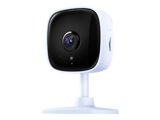
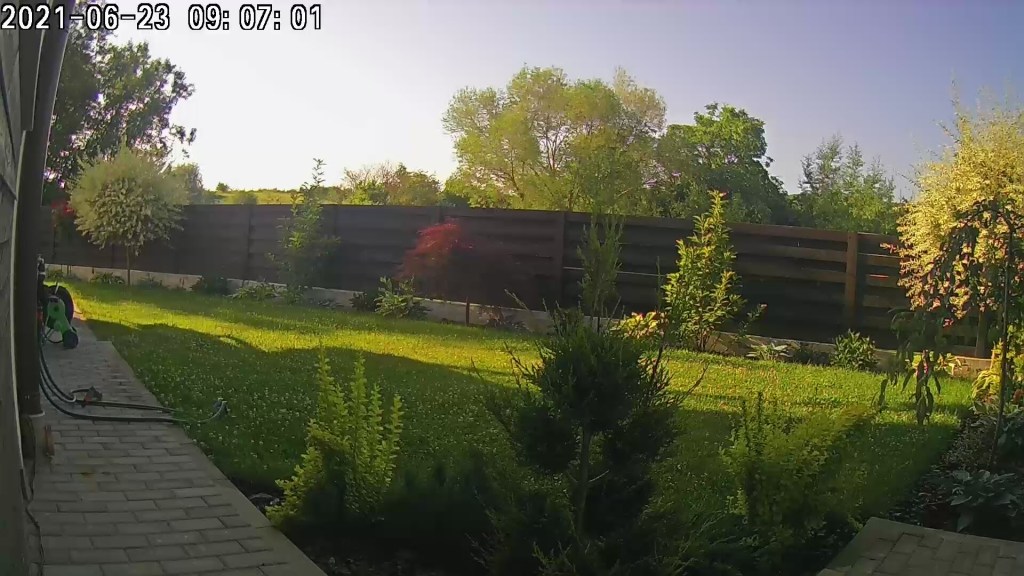
A cheapWiFi camera should be fine as I don’t want detailed monitoring or ultra HD resolution. I stumbled across the TP-Link Tapo C100 and I bought it immediately as it had a very competitive price as well – around 30$. It offers motion detection and “night vision” as well so I thought why not ?
The camera:
Pretty small device with some nice features packed in – great ! Let’s move on.
Preparing the stuff
Requirements:
Should work outside and in rainy conditions as well (moisture and all the good stuff that’s out there in the wilderness)
24h availability if possible
Low power consumption is a nice to have as well as this thing will be powered all the time
Building phase
The most awaited part – yess !!!
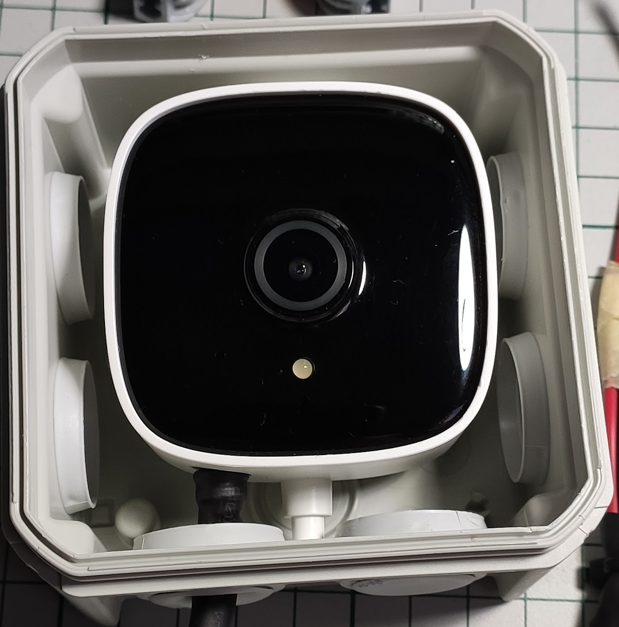
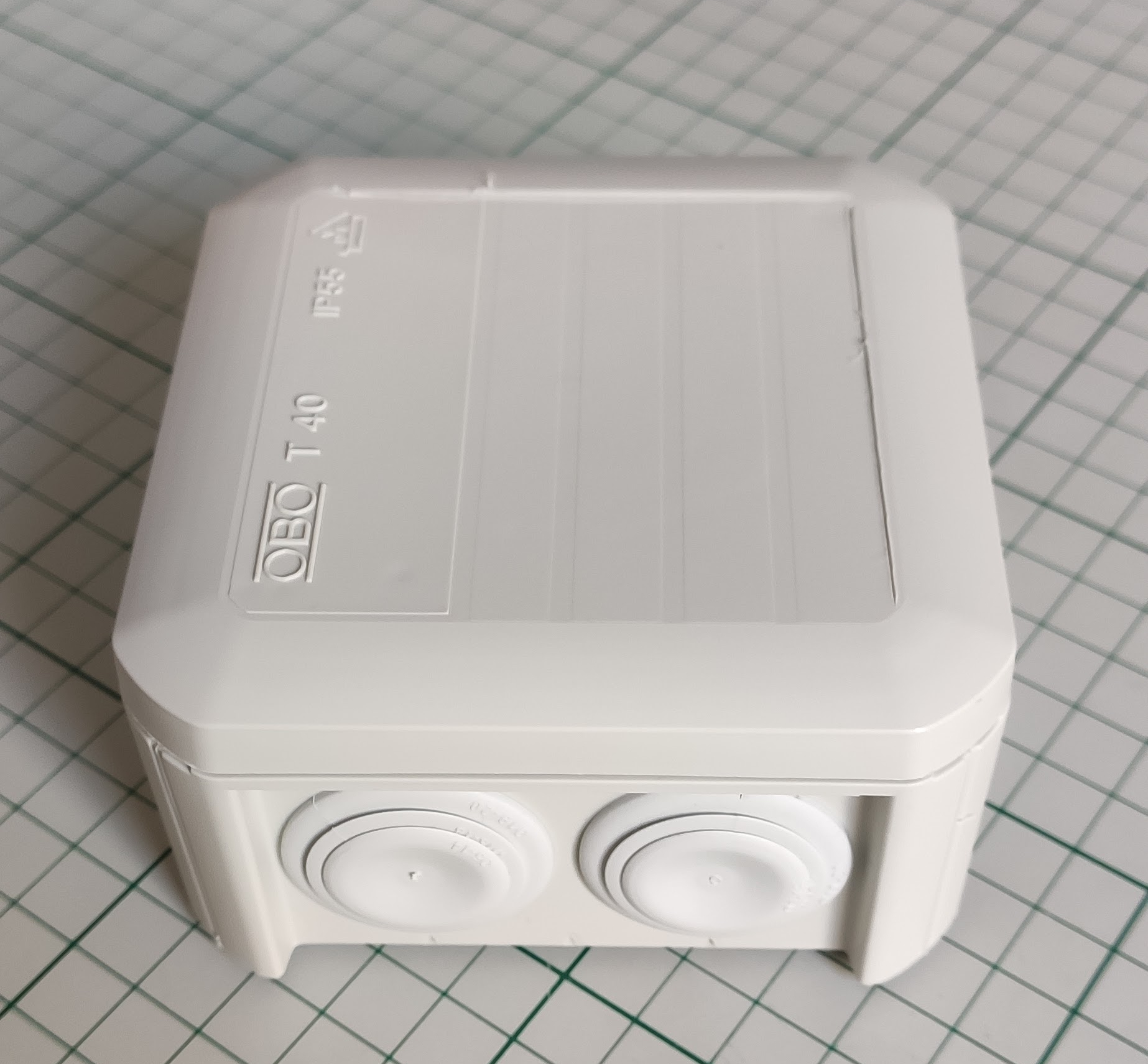
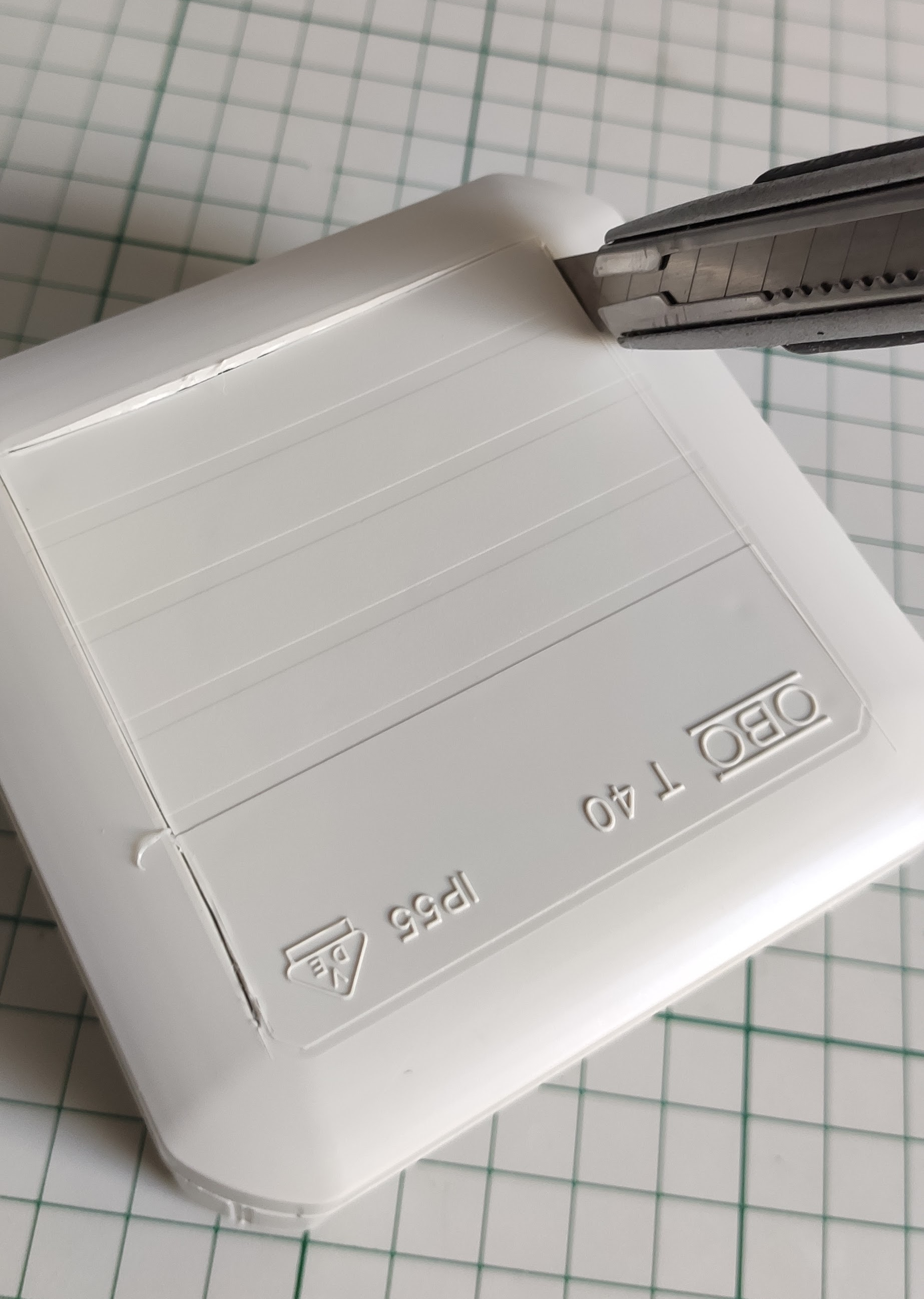
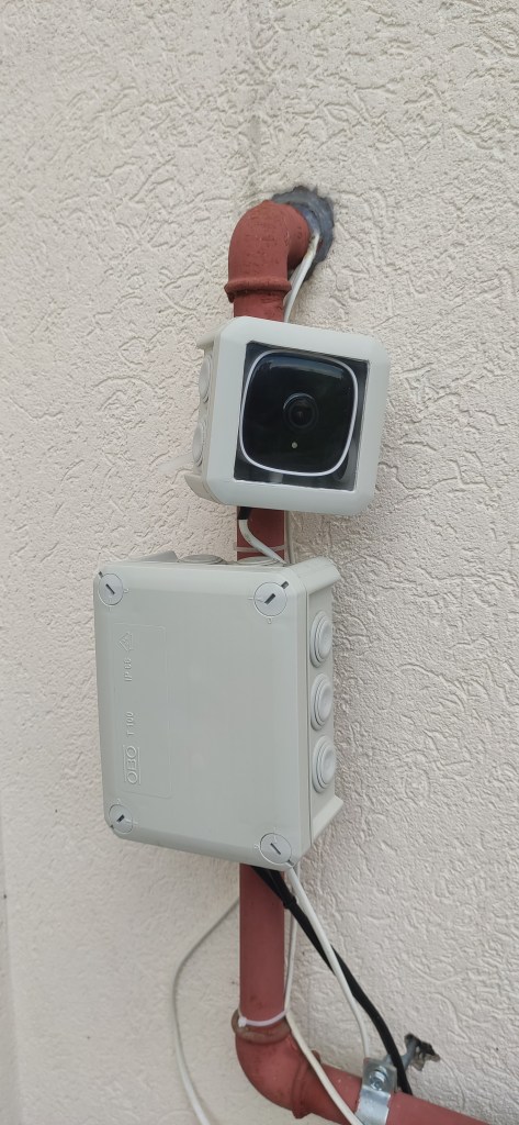
Initially I wanted a small junction box IP65 rated but I haven’t found one in the local store to fit the bill so I went with a IP55 which is not that bad after all. I don’t live in a stormy area so it should suffice theoretically – doing compromises ? We’ll see later if something goes bad – being a cheap camera I think we can accept this compromise and after all it’s not something that’s part of a vital system so yeah… let’s move on with the build.
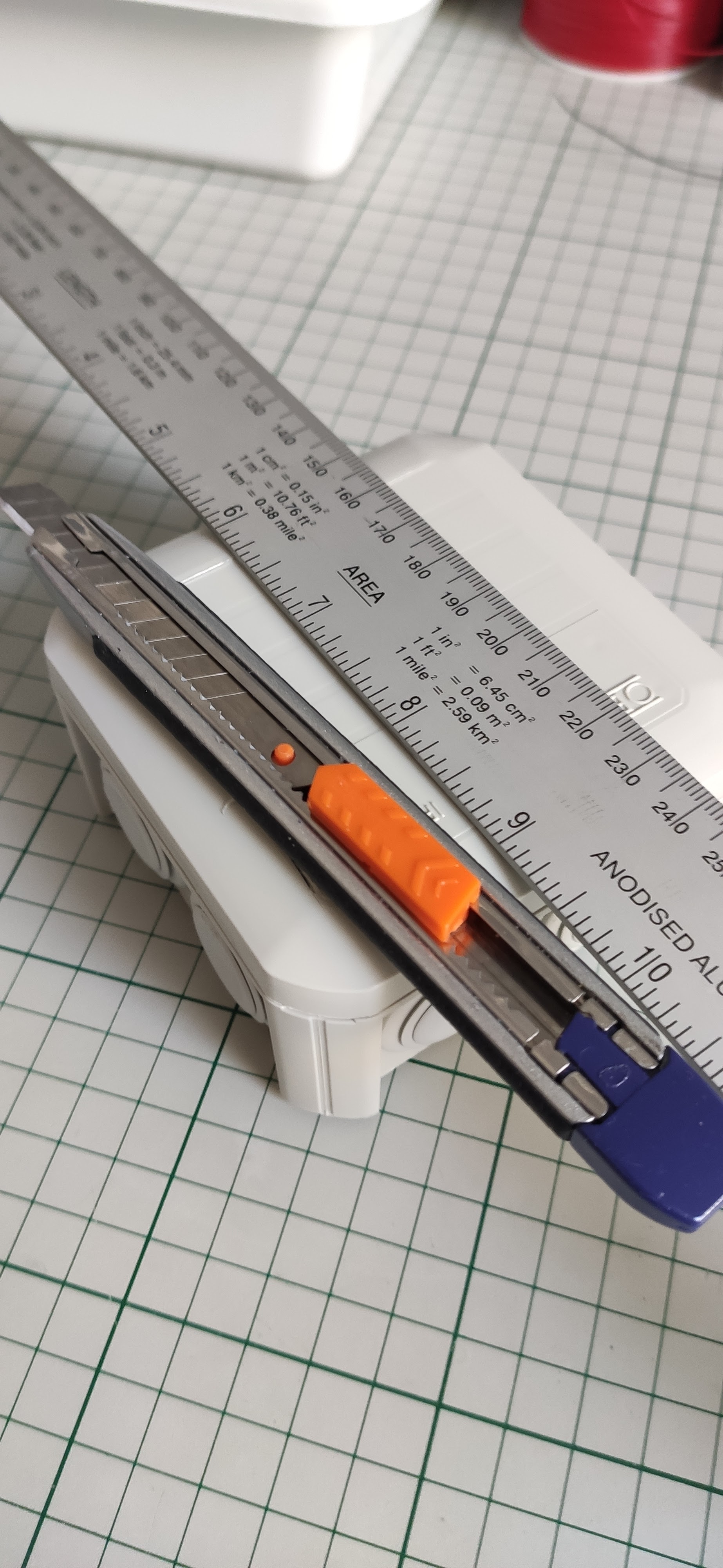
Preparing the enclosure: first let’s cut a window for the camera so that it can “see ” outside.
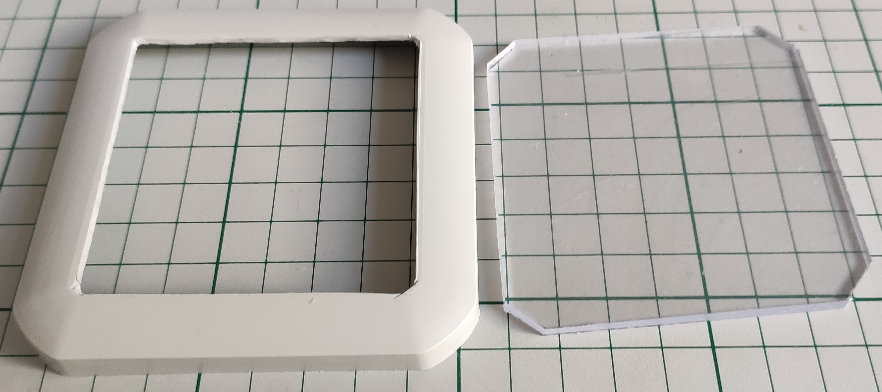
For the window and final assembly I used a piece of acrylic glass and glued it to the box lid:
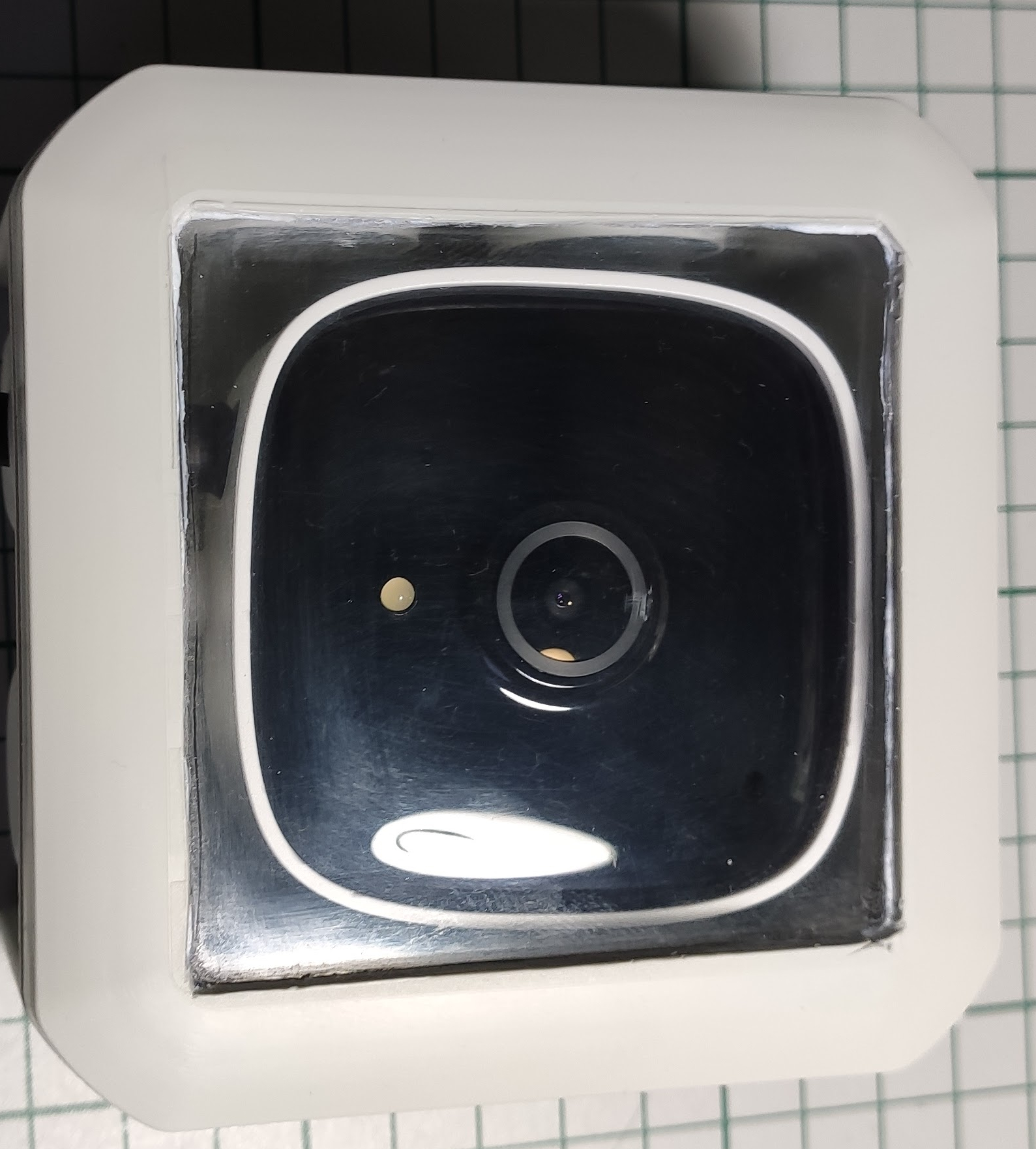
For the moisture part I added a little bag of SILICA-GEL inside the box – will it keep it dry ? We shall see …
Next after the assembly was done I had to take care of the “electric” part – here I’m talking about powering this thing. The original power supply has an output of 9V/0.6A – continuous current of course.
I already have “power” available outside in another junction box which keeps alive my sprinklers automation (another self made project that I will talk about later in another post). So all I have to do is to steal some power from there.
I did the math first in order to see if we have enough juice for all – the camera takes around 1 – 1.5W of power on average which is pretty damn low. Let’s take around 2W into consideration as a maximum.
The sprinkler valves are rated at 24Vac and 370 mA inrush, 210 mA holding as specified by the manufacturer. This means that initially one valve draws around 24V x 0.37A ~= 9W real power and then it settles to 24V x 0.21A ~= 5W. So my power supply should be able to withstand in the worst case a peak power draw of about 9W+ 2W= 11W. The previous math assumes that one valve is running at a time which happens to be my case. I have two zones that need watering but I cannot water them both at the same time because there’s not enough water pressure hence the previous mention.
Now the transformer that I bought long time ago is a TEZ30/D/24V – 30VA rated. Yes I know, I know that is apparent power and it’s not quite the real power. Depending on the load if it’s reactive or not we also have a reactive part of course. The valve solenoid is reactive obviously because it’s a solenoid so there’s reactive power present as well. The manufacturer gives us the current drawn but is it the real part or the apparent/virtual one? Not very clear – but if I remember well when talking about AC stuff and this valve is rated for the AC part I assume that’s the apparent value.
So the above power rating for the valve should be 9VA and not 9W. Apparent power is always bigger than real power so if we take this into account then with a 30VA rated transformer we’re on the safe side. I neglected the 2W of power drawn by the camera – why ? Well because is so little compared with what the rest of the circuit draws so again we’re on the safe side.
OK so my transformer delivers 24Vac which gets rectified and that gives around 34 -35V of DC voltage. I need a DC-DC converter of course because it’s more efficient when it comes to lowering voltages of this level of magnitude. If using a classic linear voltage regulator to get from 35V to 9V oh well… that means (35V – 9V) x 0.2A = 5W !! Ouch that’s a lot for a linear voltage regulator to withstand – lots of heat – not good ! And another important aspect: it dissipates lots of power that’s not needed – much more than the load (camera) requires !!!
Note:
The 0.2A from above was computed from observation (I could insert an ammeter in the real circuit and get the exact value but I was lazy). I noticed that the camera draws about 60mA when powered via the DC-DC converter from a 24Vdc source which means: 24V x 0.06A ~= 1.44W. This translates to a current draw on the 9V input from the camera of: 1.44W/ 9V ~= 0.16A and I rounded up the value just to consider the worst case OK?
Now you know why I made the assumption that the camera draws around 1.5W of power on average – let’s not consider the power loss introduced by the DC-DC converter shall we? … because it’s smaller and we all know that DC-DC converters are pretty efficient ( well not on the whole range of input vs output voltages of course but again let’s keep things simple).
Phew… a lot of math and I don’t like math very much to be honest but it seems to be a necessary thing.
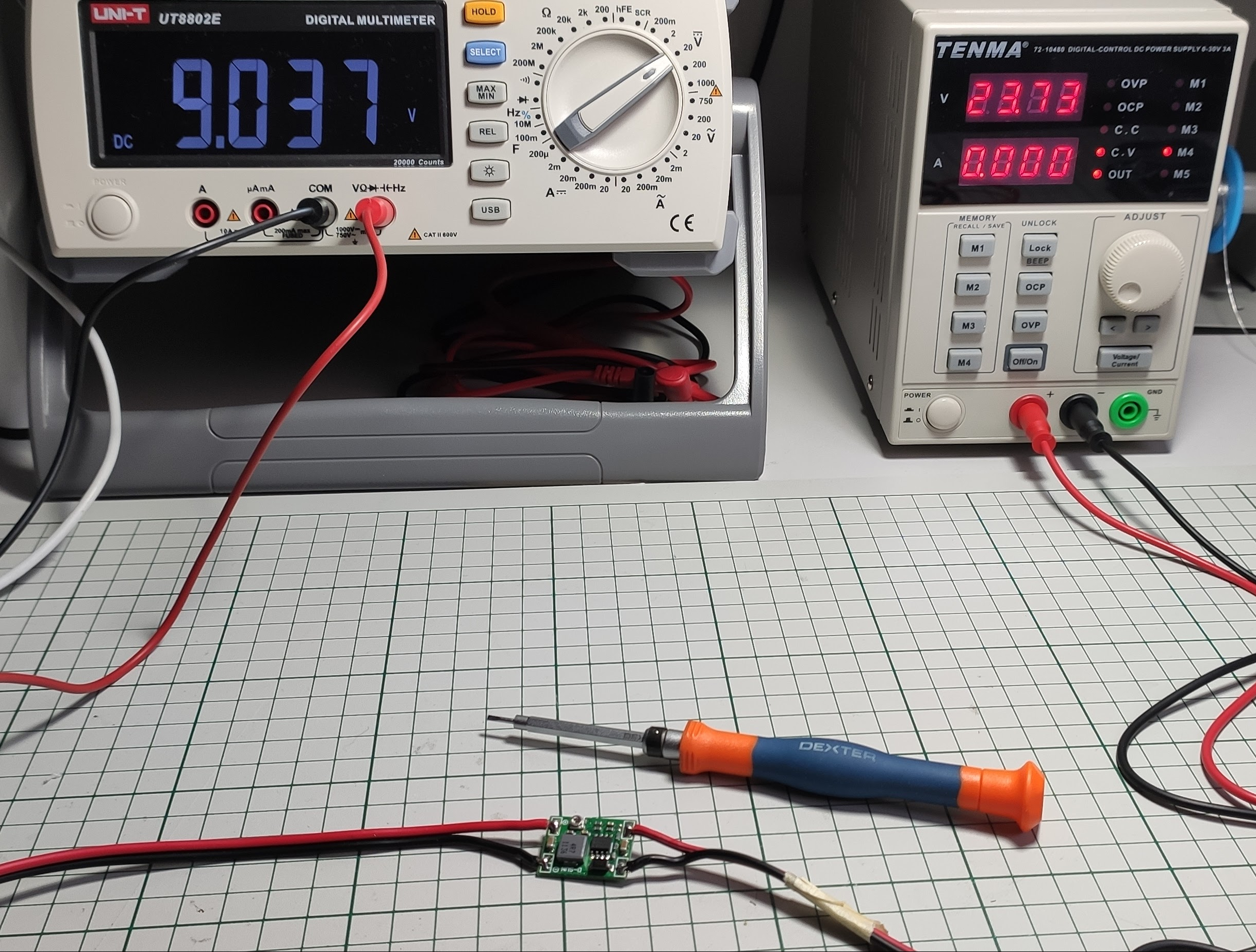
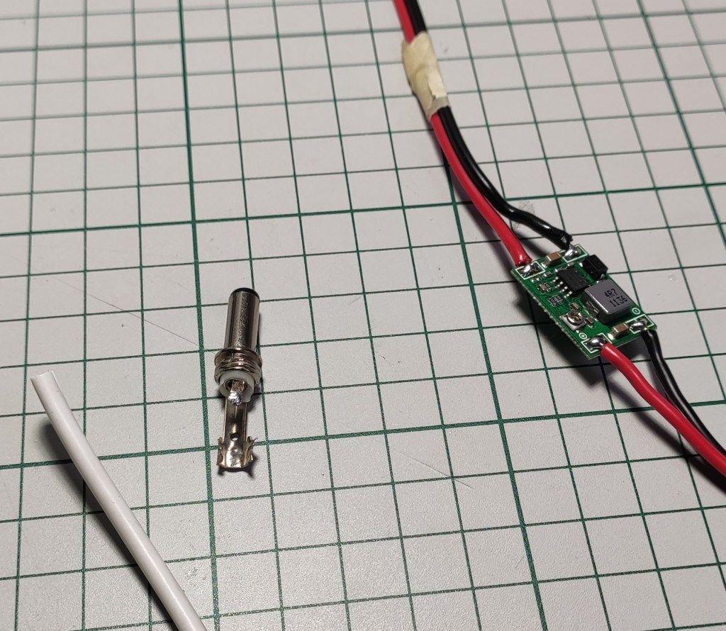
Tuning the DC-DC converter output to 9V:
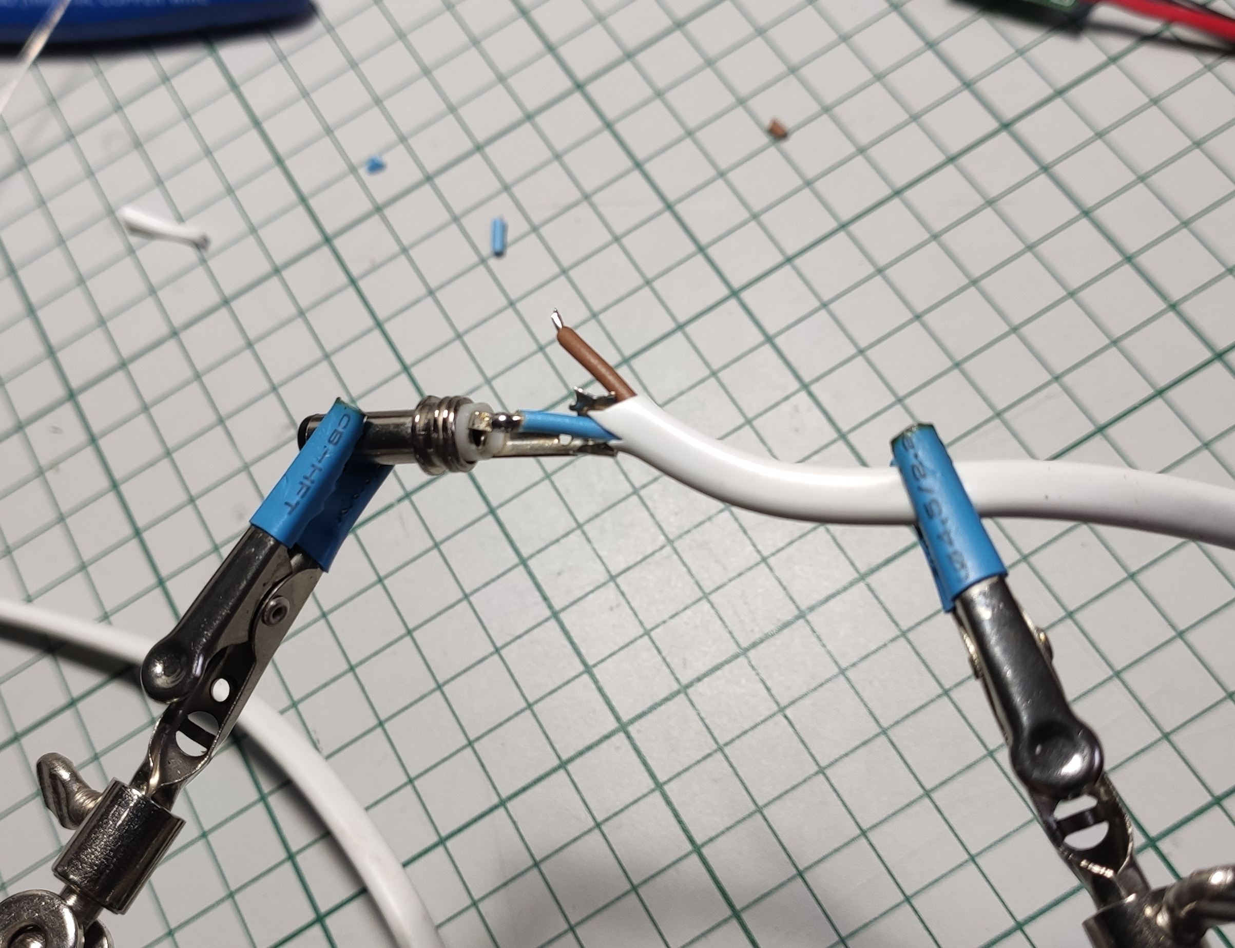
And the final piece – soldering the barrel connector:
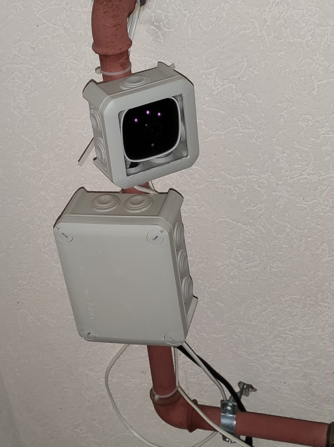
We’re getting close now to (on the right – night mode enabled) – ignore that little mess of wires for now:
The “software” part
The initial setup must be accomplished via the official Tapo application which includes: connecting to your home WiFi, setting the camera name, etc. After this part and/or other tweaks that you want to make inside the app the next part is the Home Assistant integration. The Tapo application is still required as far as I know if you want to perform firmware updates in the future and other stuff that is not accessible outside the app.
For the Home Assistant integration you need HACS installed and configured first. Then the Tapo: Cameras Controlcustom component must be added and configured. All the required steps are documented on the official Github page.
Note:
A camera account is required in order for the Home Assistant integration to work. This can be accomplished inside the Tapo application in the advanced camera settings (tap the camera -> the gear icon in the upper right corner -> advanced settings – > camera account). This is not the cloud account that you configured for logging into the Tapo application.
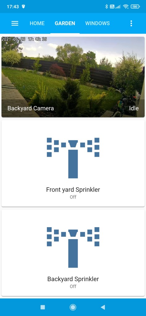
And the final result – live streaming:
I also succeeded to add the video stream inside my “Garden” view from the Home Assistant dashboard and it works quite nice (it has a little bit of latency compared with the Tapo application but it’s OK as I don’t need details in this case).
Conclusion
I can further add other automation on top of it if desired because I also have motion detection available so… all in all I’m happy with the build and I consider it a success.
So if we take this metaphor and rearrange it a little bit then this means that I can also say that “The windows are the eyes to my home soul” ?
Motivation
Before getting to the point I wonder how many of you and more important how many times when you left home you asked yourself:
“Oh… is the Living Room window closed ?” or “is the Attic Window closed ? ”
Because it may rain and oh well… you know the consequences. I for sure did and not just once. So here we go …
Main goals
Have a way to get notified when you leave home that you forgot to close window X or Y
Small enough and battery powered is a must
Wireless of course
Good coverage required as well (for big houses)
No glitches or false alarms please !
Hardware implementation
We need first a piece of hardware to run this of course. But what options are available?
Here are a few:
Buy a ready made solution – the easiest of course. But it can also be expensive and maybe hard to maintain over a long time and also very likely to get into a “vendor locked” situation – not good!
Build it yourself ! Yes !!! This is the part that I like the most.
A mix of the above – wait a little bit… What ???
And again I will get straight to the point and say that I decided in the end to go with the 3rd option – yes a mixture which turned out to work really well (even beyond my own expectations).
But until then I will tell you everything that I’ve been through: my experiments, challenges and so on …
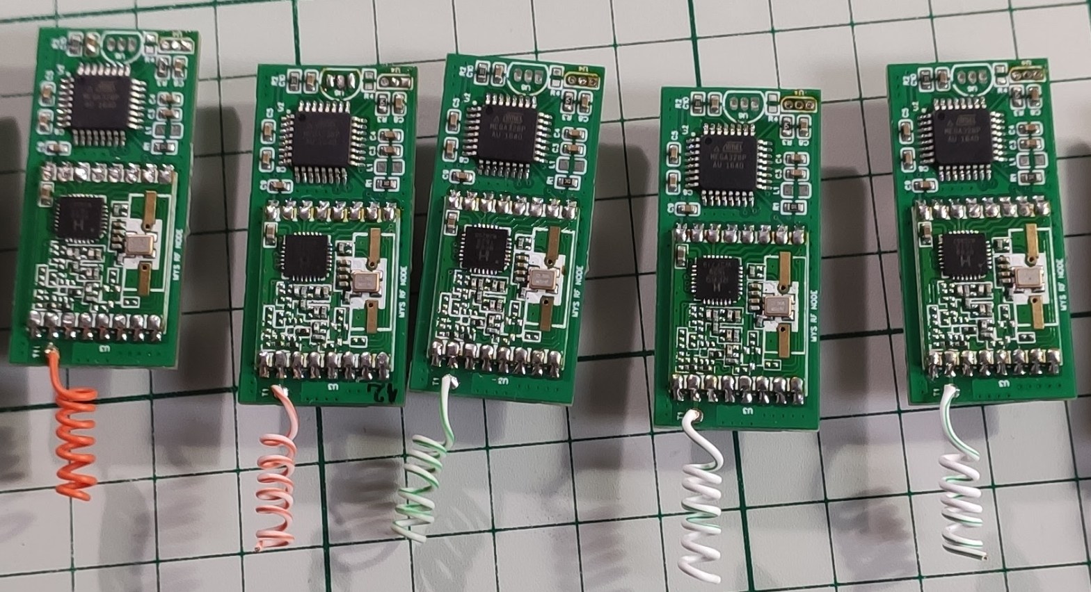
Let me present now the candidates:
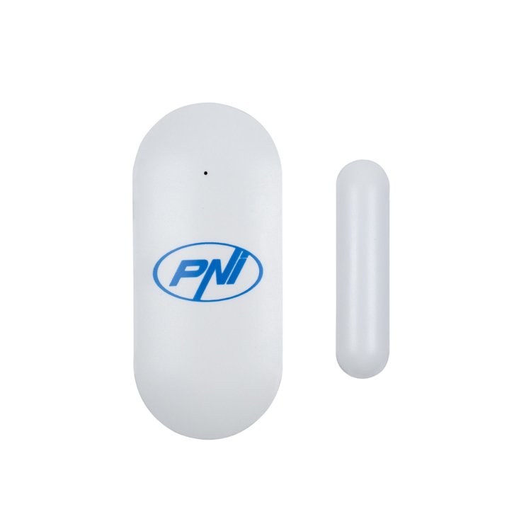
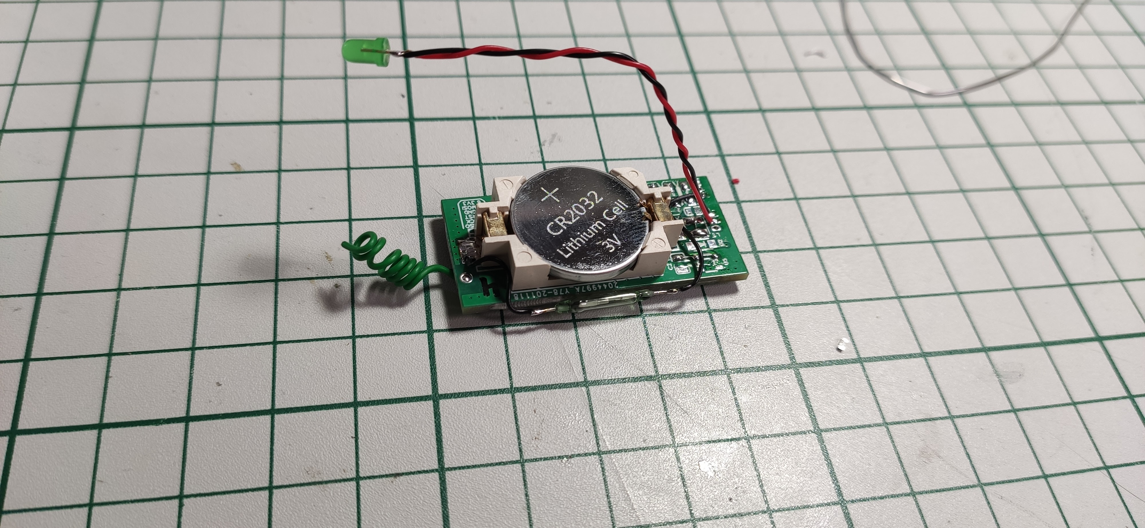
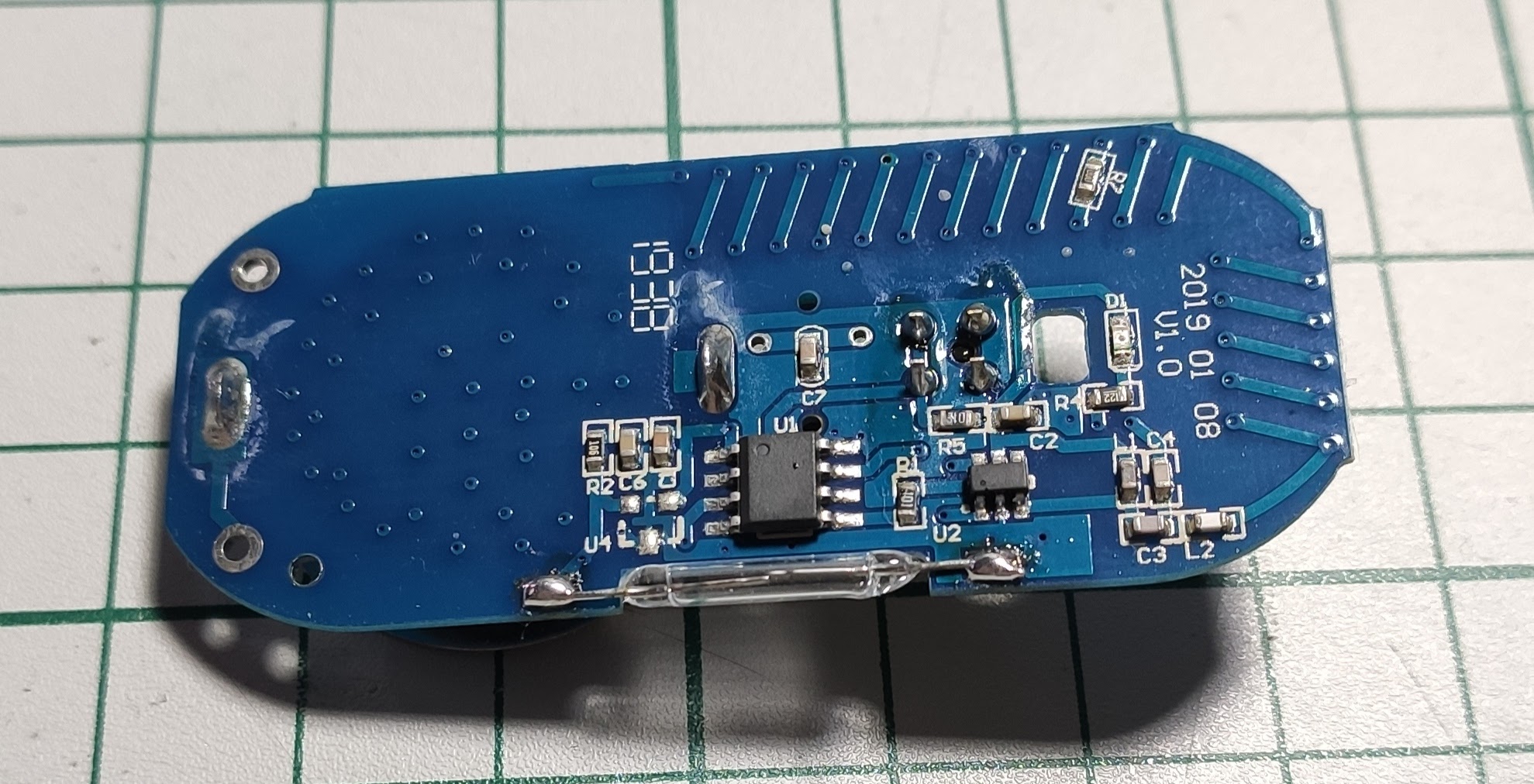
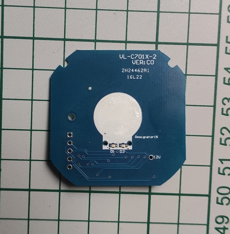
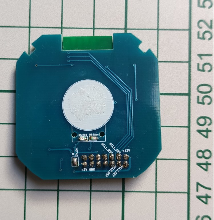
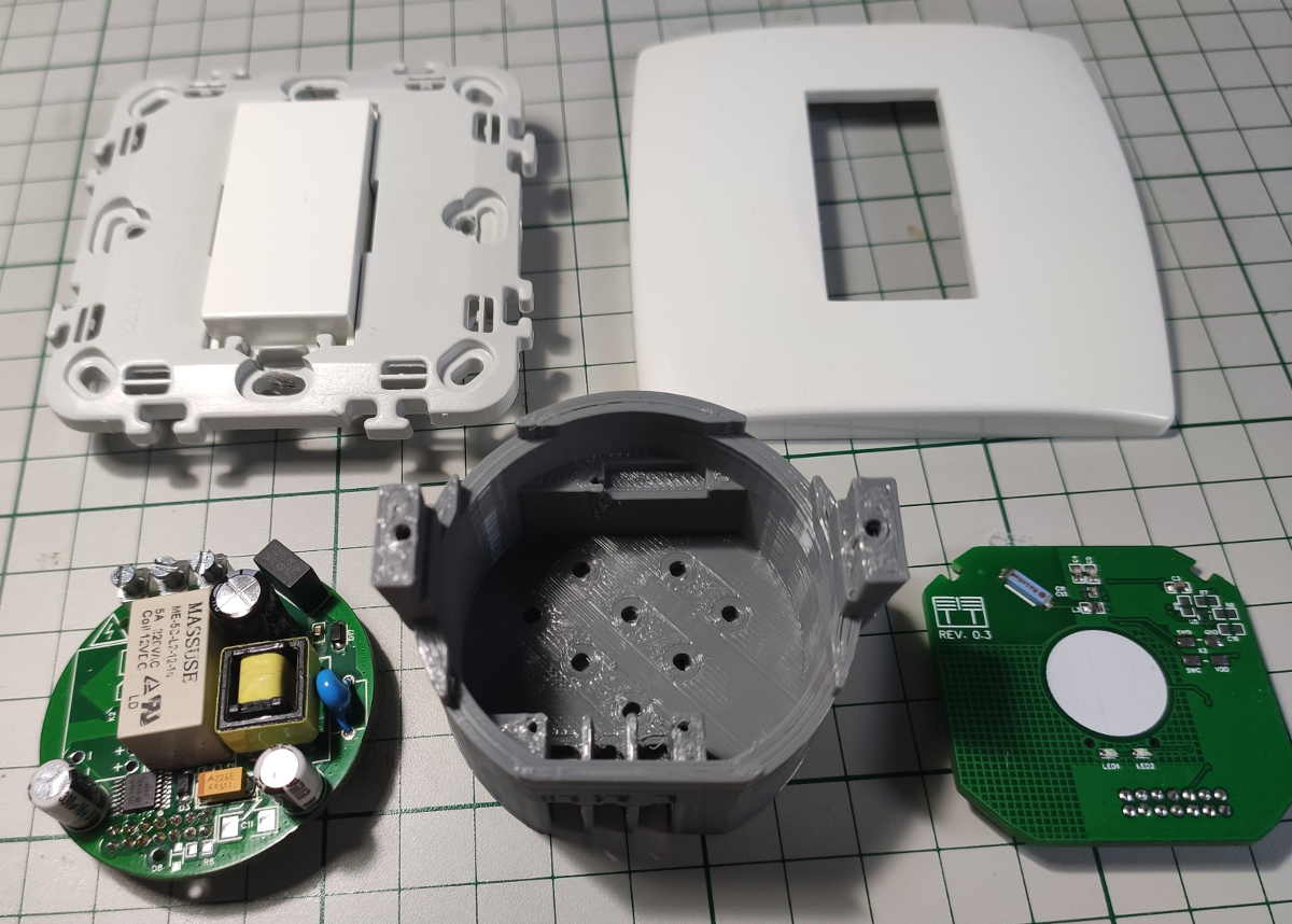
On the left side is the sensor that I bought from the store aka the PNI HS002 and on the right side is the custom board that I made myself to replace the original one. Why ? Well let me give you a little bit of context first.
How the story began actually
Initially I wanted to have a quick solution and something that just works out of the box. Sometimes I am lazy and not enough motivated to build something on my own or go via the DIY route and that’s why – “comprehende” ?
So there I was and bought 15 pieces of this battery powered “magnetic window sensor”. But later on it proved to be not very reliable and then I started to cry – well not in reality. In reality I started to get angry and said to myself: why did I trust this vendor and bought all of this sh1t ?? It wasn’t very expensive but still … why the hell some things even exist ? Just to steal your money and my precious time because let’s face it – time is more precious than anything else in this ever evolving world and I don’t care if you really agree or not with me because this is a real fact – period!
Of course the mistake is mine because I was rushing things out and never let this “thing” run enough so that I can test it and review it in more depth so to speak. Why? Because I don’t have time or patience sometimes so here we go again and touch the “time is precious” part or better to say “time is something that I cannot afford sometimes”. Who the hell created “time” in the first place anyway?
Ok… enough is enough. Now let’s try to calm down and fix the this damn situation because we’re engineers right? We like to repair stuff but more than that to build stuff – YESS ! That’s the spirit !
First tentative
If you have physical access to a system you own it!
Believe me or not the above is very true in most if not all of the cases. I mean how many of you had to repair a PC and had physical access to the unit and then used its CDROM drive in the old days or a USB stick nowadays. If I have physical access to a machine (PC in this case) I can do anything with it: I can boot it using a custom bootable CD or USB stick and then have access to the hard drive data (if not encrypted – a lucky situation) and then reset passwords or whatever I like.
Now getting back to our window sensor. In this case I did a little bit of reverse engineering and noticed that it has the following building blocks:
ASK transmitter working on 433MHz
Remote control encoder IC – this is like the classic PT2262 or the like
Reed sensor (a switch that is sensitive to a magnetic field)
All of the above can be observed on the original board:
the big bug with 8 pins is the encoder IC
the small bug with 6 pins is the ASK modulator and RF transmitter
the REED sensor in that glass balloon at the edge of the board
Then I said: OK we can integrate this thing very easy with my home automation system via MQTT using OpenMQTTGateway which is a very cool project btw (I made a few contributions to it – some PR’s to address some issues on their Github repo).
So there I was and started integrating the OpenMQTTGateway project with these sensors and it worked… to some extent.
But I wasn’t very happy after a while because:
Range was an issue and this is the most disturbing part when it comes to building sensor networks and not only
False readings which means that random sensors started to appear in Home Assistant (because I love and use Home Assistant btw). This was because of the unacceptable noise present on the RF medium and ASK demodulation doesn’t deal very well with it – remember the days when listening to AM radio stations ? So yeah… unreliable data which is even worst …
I forgot to mention about the hardware part used to power the OpenMQTTGateway project.
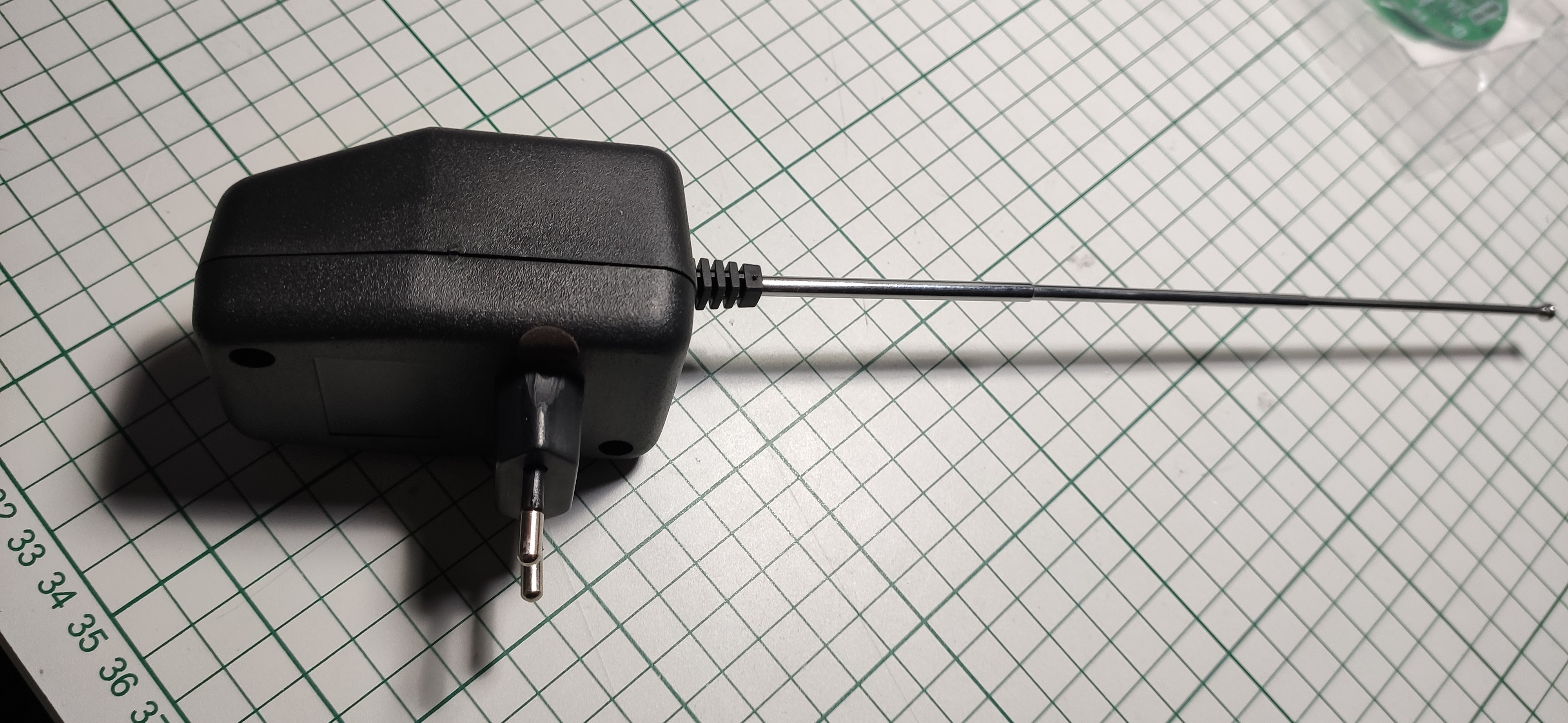
Here are the main components involved:
ESP32 board for the WiFi part (bought from AliExpress long time ago)
433MHz ASK receiver (bought from the same place)
5V/1Apower supply – this was “ripped” apart from a cheap Phone charger
Power supply box
Telescopic antenna for the ASK receiver
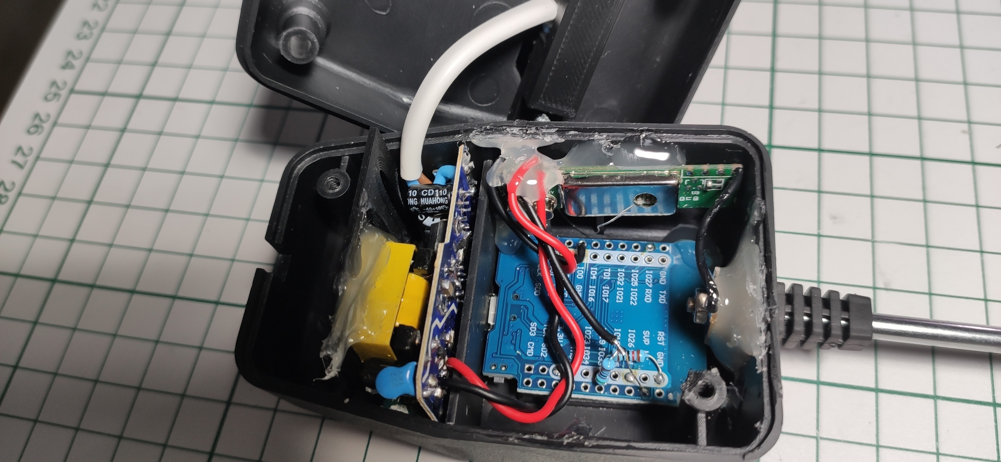
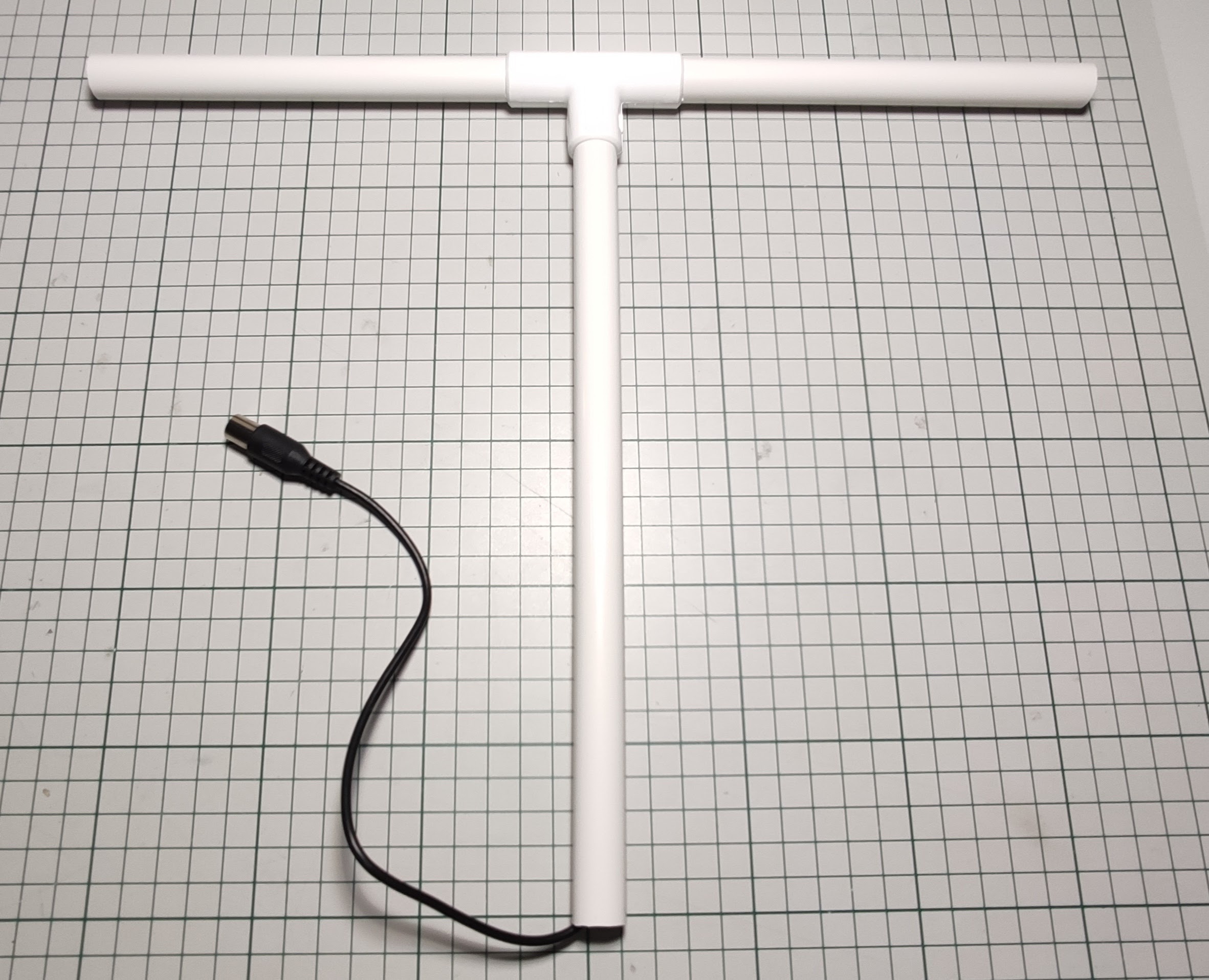
Some pictures with the final build of which I was very pleased:
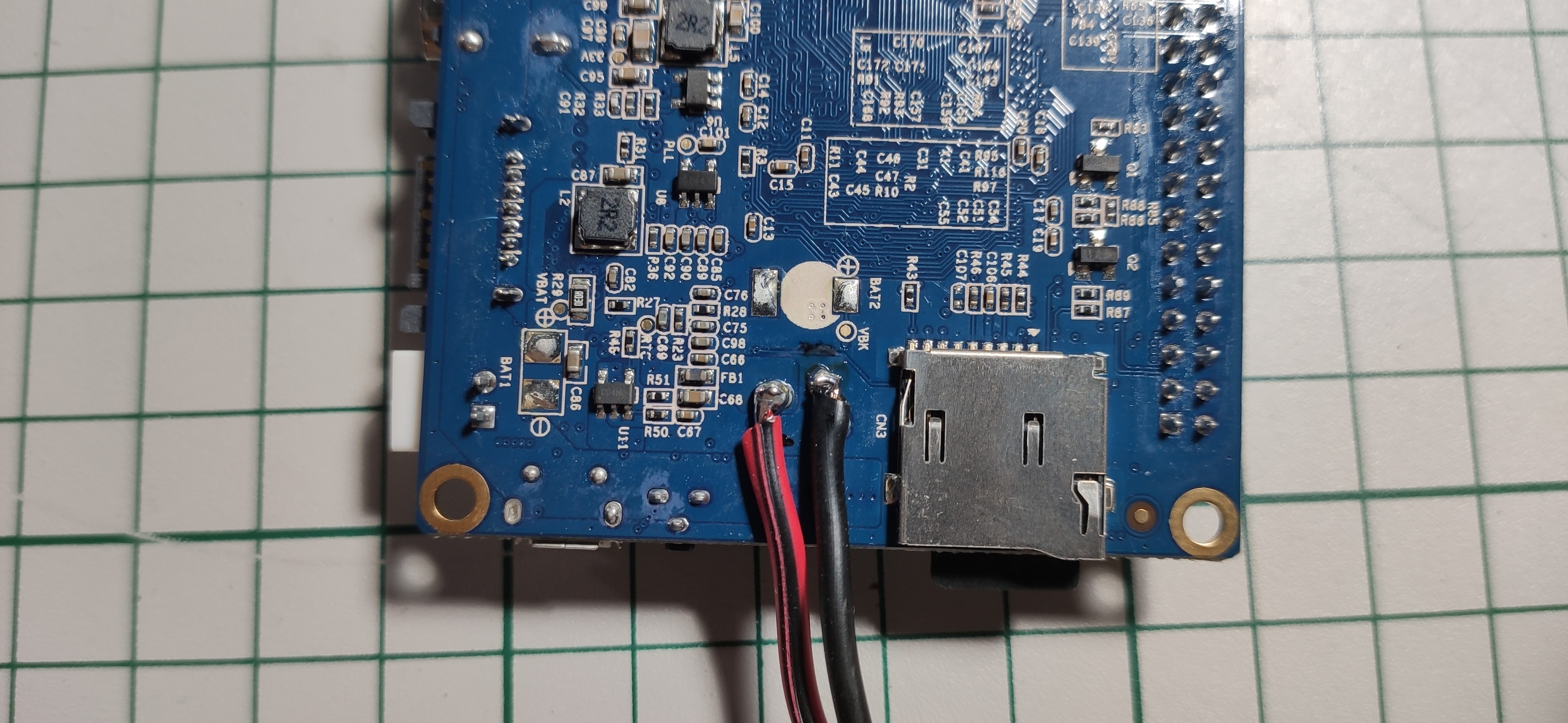
You can see the main WiFi board – the blue one that’s near and a little bit under the telescopic antenna. The 433MHz ASK receiver is the green board with a metallic cover used for shielding. And the power supply board is on the left side where the mains cable also is (the white one that’s much more thicker). There are also 2 blue resistors (barely noticeable in the picture) used to form a voltage divider because I have to power the ASK receiver with 5V to work and the WiFi module accepts 3.3V levels only on the pin used to read the ASK signal after demodulation. For decoding the signal OpenMQTTGateway uses the almighty ArduinoRCSwitchlibrary.
Second tentative
I revisited this project after a while and I thought: hey maybe the transmission channel is not very reliable because of a bad antenna design ! And indeed it was for Christ sake !
Let me start with a veryimportantnote first:
Never forget tocheck if the antenna is built and matched accordingly. Like in a previous post when I was talking about the importance of a power supply in a electronic circuit likewise in this case theantennais a very important part of every radio system from this planet !
Yes you heard me well and I hope you did! If a circuit has a poor power supply then the same applies to a radio system with a bad antenna – period ! End of story ! And of course both are key points that you and I need not to forget.
Why the first hardware build was not very reliable on the 433MHz part? Well because of the amazing telescopic antenna. Yes it’s an amazing antenna and it brings me back some old memories but it’s not so amazing when it’s attached to my home automation system. It’s an omnidirectional antenna and that’s OK because we don’t want to track something so I don’t need an unidirectional one but still… there are much better alternatives.
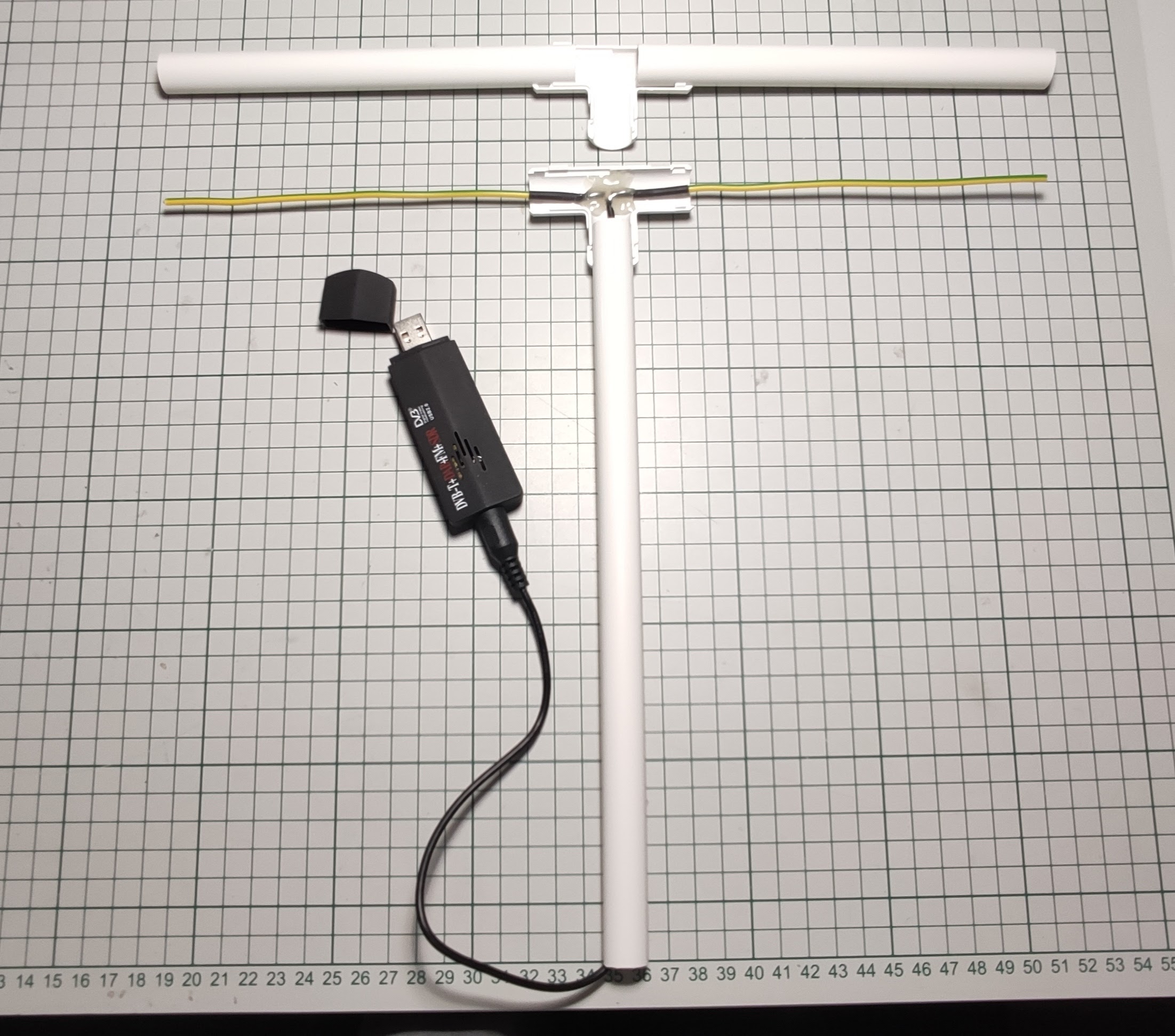
Now of course I’m not a RF expert and nor an antenna expert as well but I do have some basic understanding of the essentials so to speak. Oh and there are so many factors that can drag down the RF link budget but let’s keep it simple now and say that I decided to go with a simple dipole antenna and a SDR module. Yes – Software Defined Radios are so cool and powerful !
I remembered that I bought a SDR some time ago and it was only collecting dust so I said why not give it a shot ?
Here are some pictures with the new and much better antenna build. The SDR module is there as well.
The dipole antenna is a λ/4 build and should have an impedance of 50 ohm (well somewhere around that value anyway). I didn’t had a VNA (Vector Network Analyzer) around at that time but I do have one now and I just need to get into the habit to use this thing. It’s a very useful device to have in the lab if you’re into radios and antennas stuff.
Then I hooked this thing into my computer and used the so cool Node-RED project to drive it. I found a Node-RED plugin or better to say “node” which allows me to use it very easily and in no time I was playing withe the SDR and getting data after tuning on the 433MHz radio frequency.
I was amazed on how easy is to spy and even decode data present “on the air”: wireless thermometers, garage door openers and so on – isn’t that cool? Well it is but not legal in some cases. In the end it depends on what you do with that data. If you use it for your personal gain as to hack someone’s garage for example then yes it’s illegal and all that. But how does it know to decode signals? The answer is very simple:rtl_433.
OK enough playing/tinkering let’s get to our own window sensors. I made a really quick project via Node-RED and inserted a rtl_433 node then some string parsing and publishing via MQTT to Home Assistant – yes it’s that simple with Node-RED.
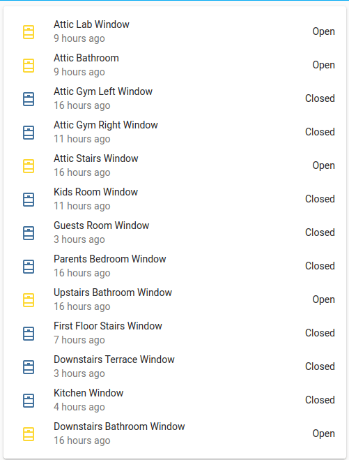
I managed to get the required data into Home Assistant and also set up a dashboard for the sensors like seen below (forgot to mention but those sensors are reporting battery state as well which is nice):
Oh and yes range was increased considerably with the new antenna design and the SDR device which has better RX sensitivity – success!
Still I wasn’t very satisfied or not quite there … Oh wait you may say – this guy is really crazy or what? I mean what can you ask for more ? What the hell is wrong with you ?
As the title pretty much says I was wondering and also wanted to try and see if I can build my own Kubernetes cluster using some ARM boards that I had laying around for some time now.
Can they do something more useful rather than collecting dust? We shall see …
Main goals
Build a cluster from spare parts – doh, that’s obvious …
Learn more about this new kid on the block – Kubernetes
The setup
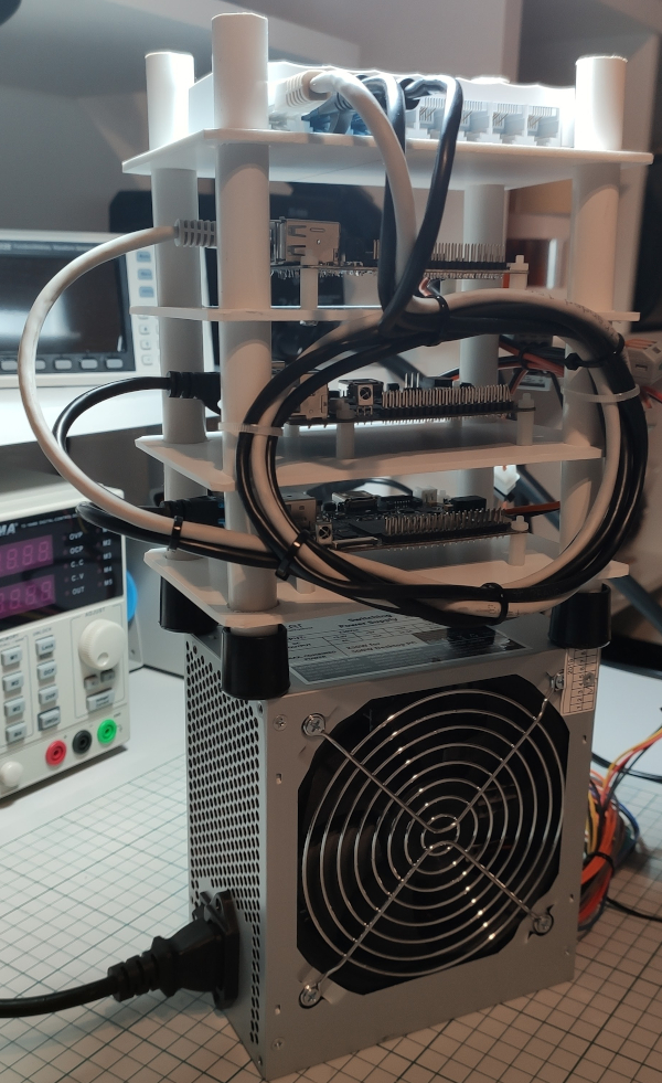
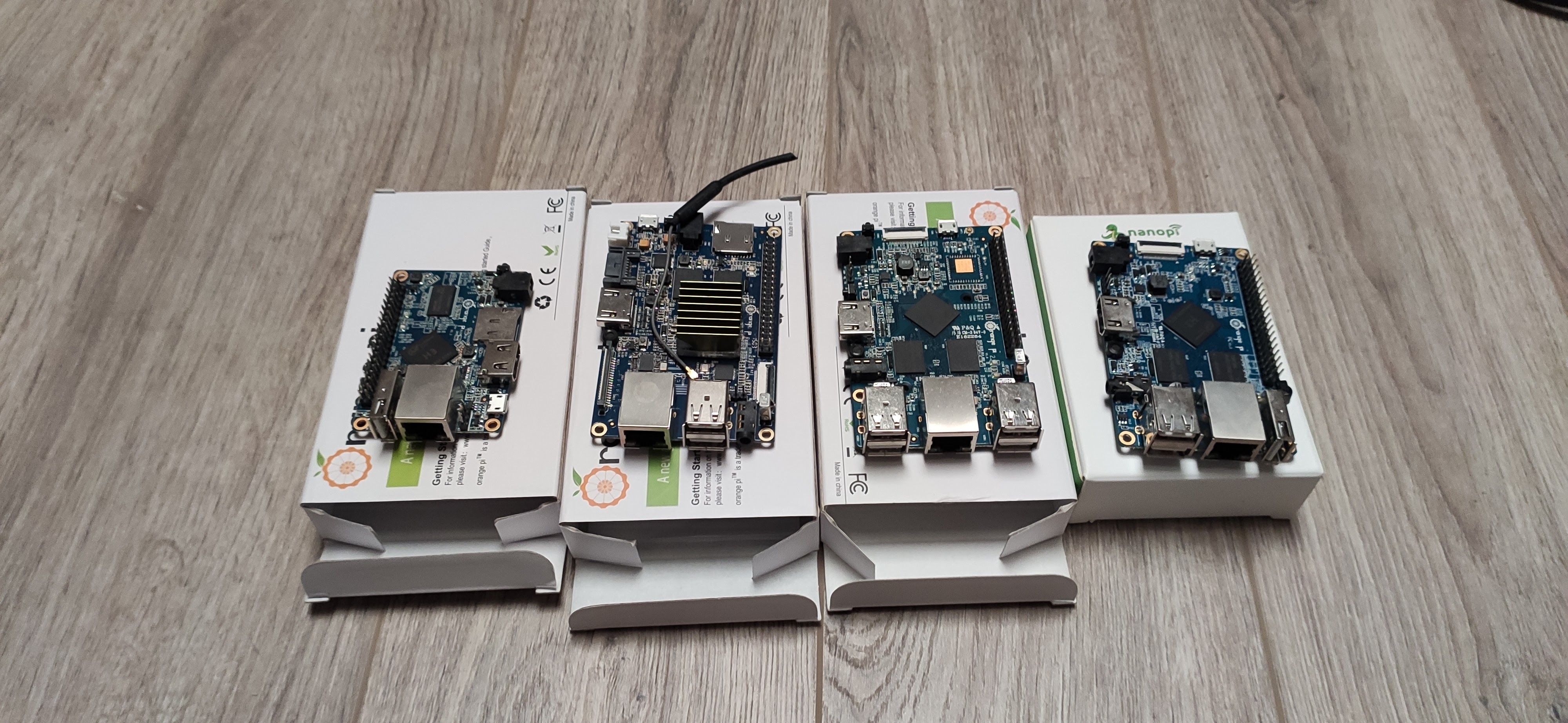
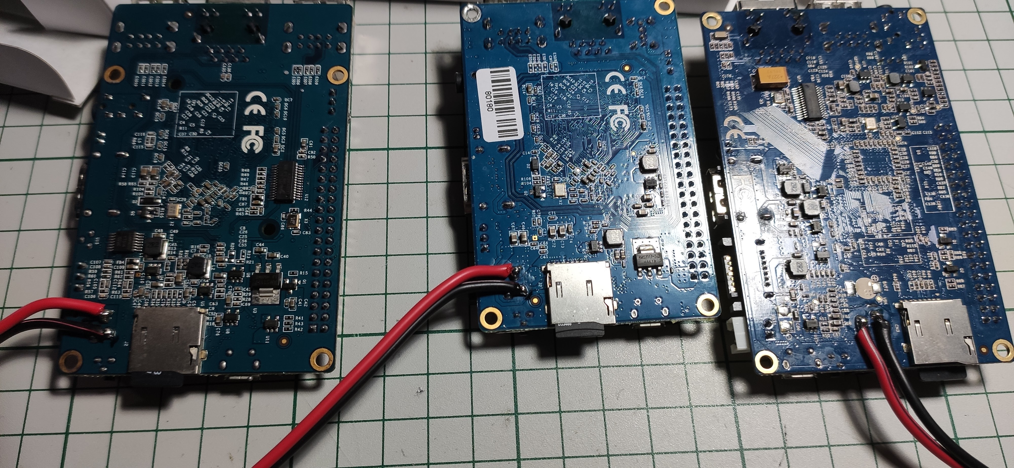
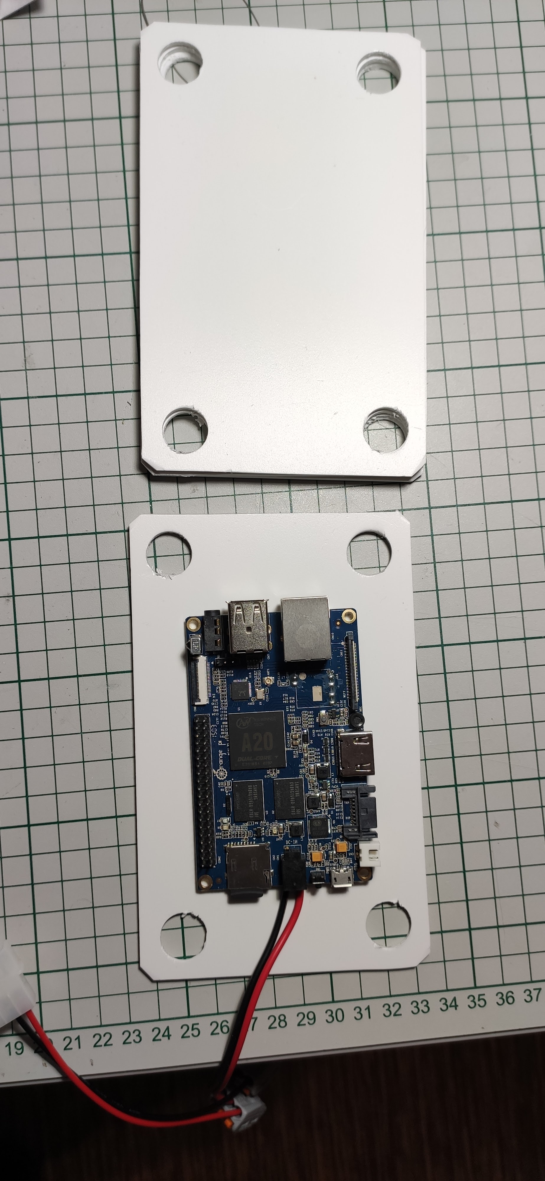
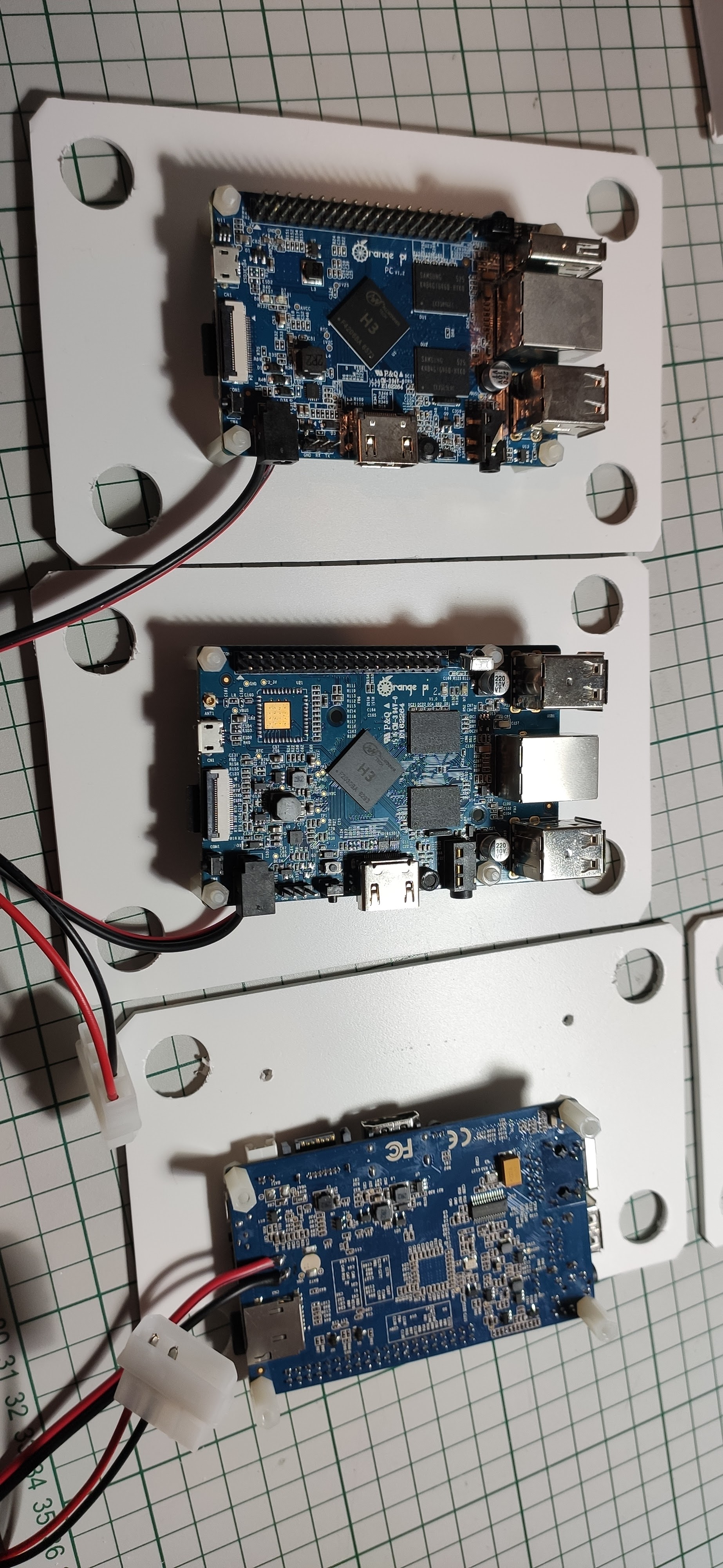
Some OrangePi boards bought from AliExpress long time ago. Funny the name though – they are actually clones (well, more or less) of the now ubiquitous Raspberry PI boards.
I only picked 3 of them for now and started building the rack (although there are 4 in the picture above). Of course we can expand the cluster if needed in the future but for now let’s start small and see how it behaves first shall we?
The building phase
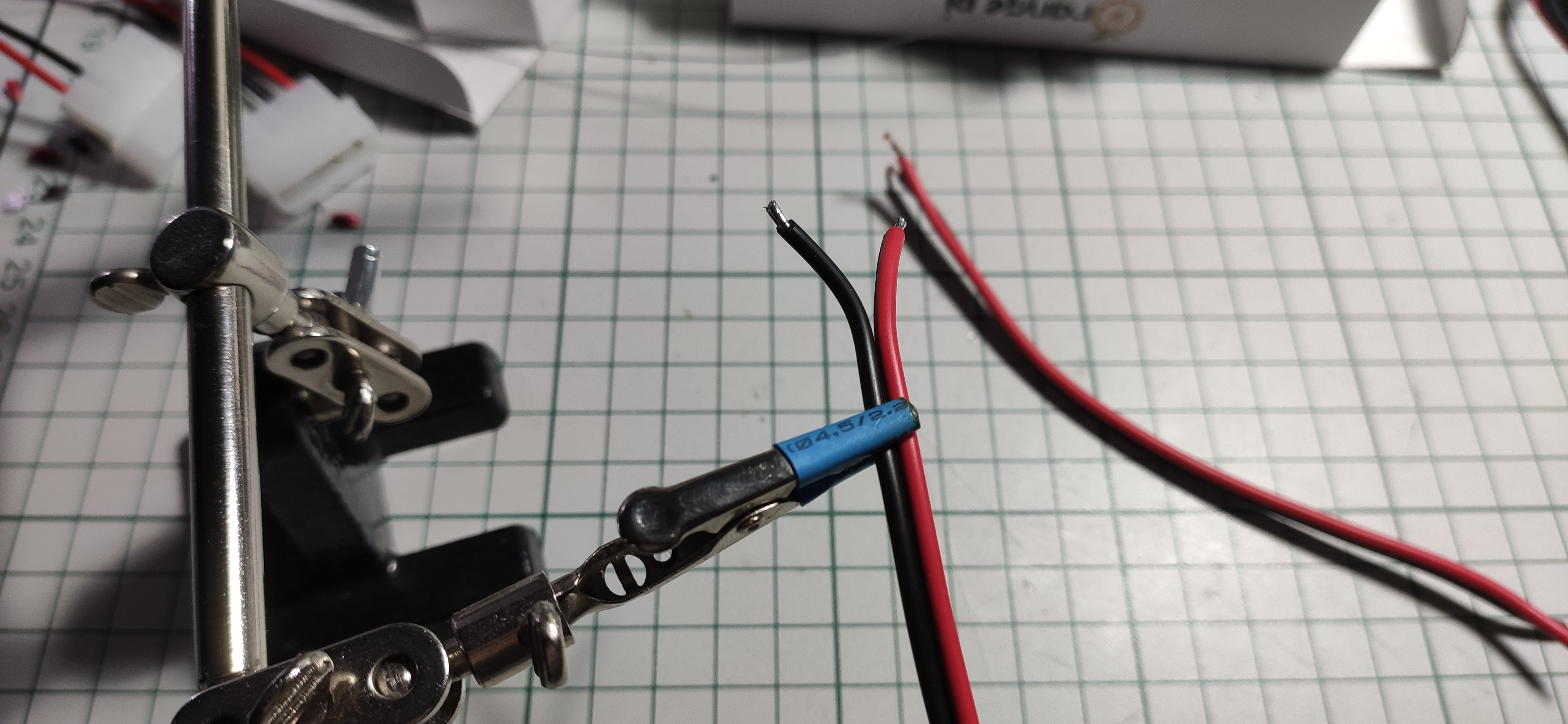
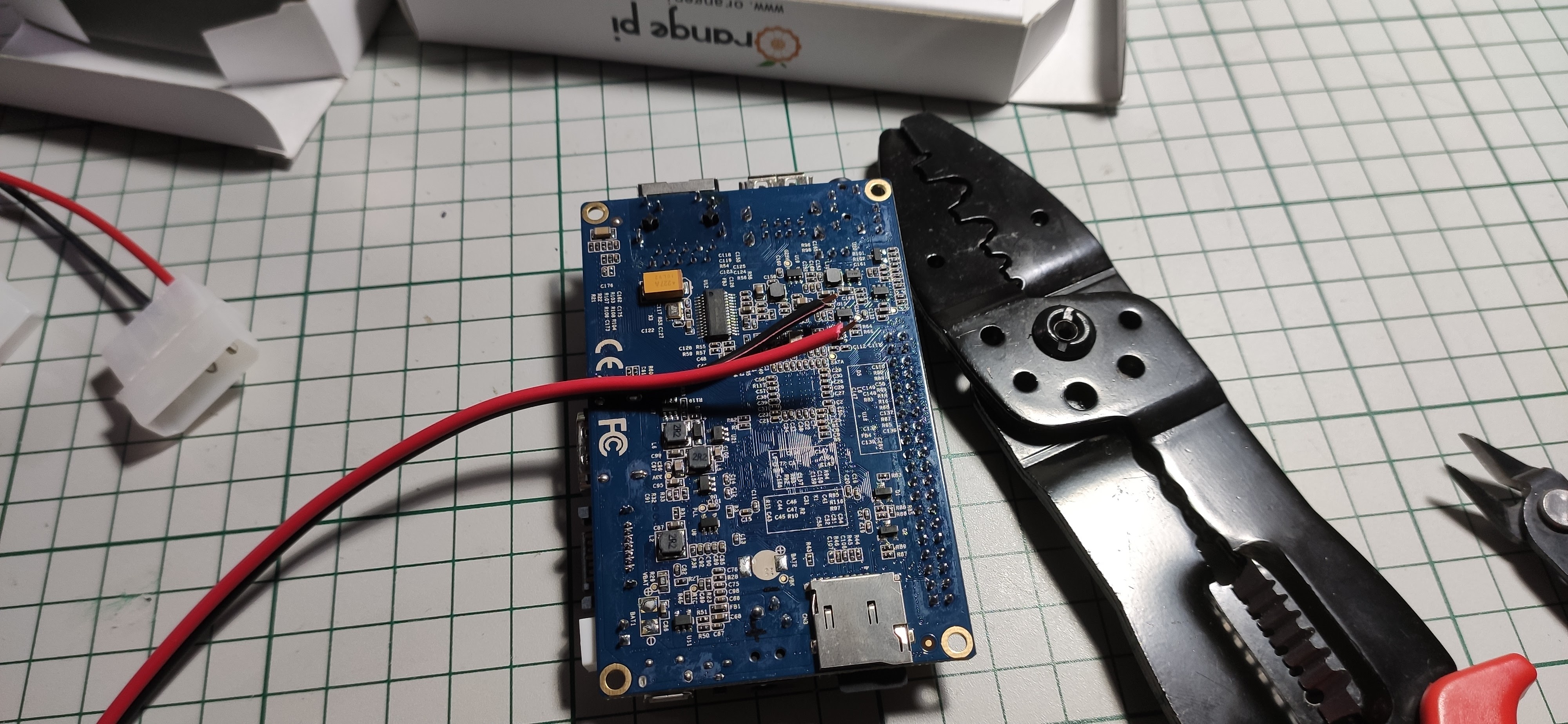
First, some soldering for the “power plane“. Each board requires a barrel connector for powering with 5V/2A but I had only one around so I decided to solder some wires on the back side because yeah, I was lazy and didn’t want to go to the hardware store. And please bear with me as everything went just fine and nobody or nothing suffered injuries – here I mean the boards themselves. It’s not the first time when doing soldering and the soldering iron is my best friend of course …
OK, some pictures now:
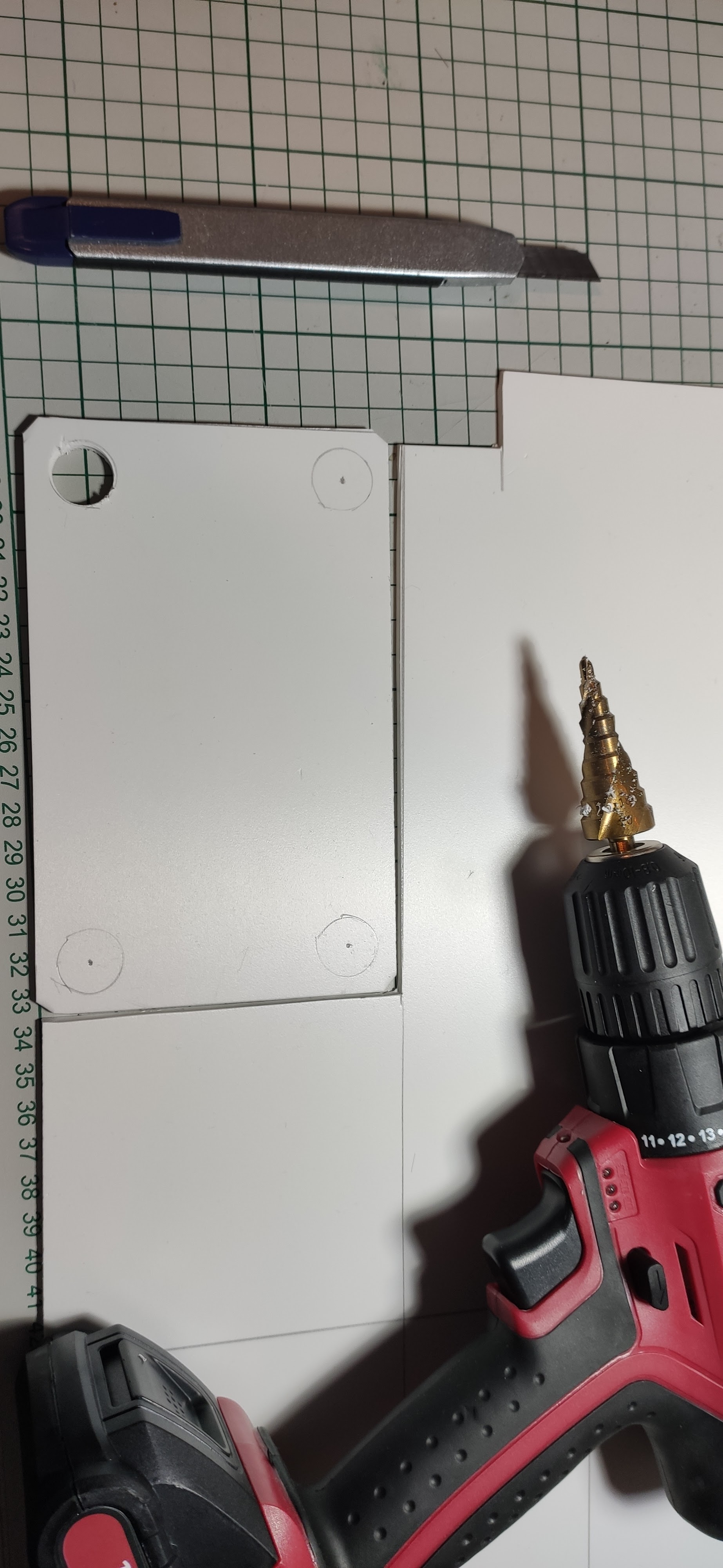
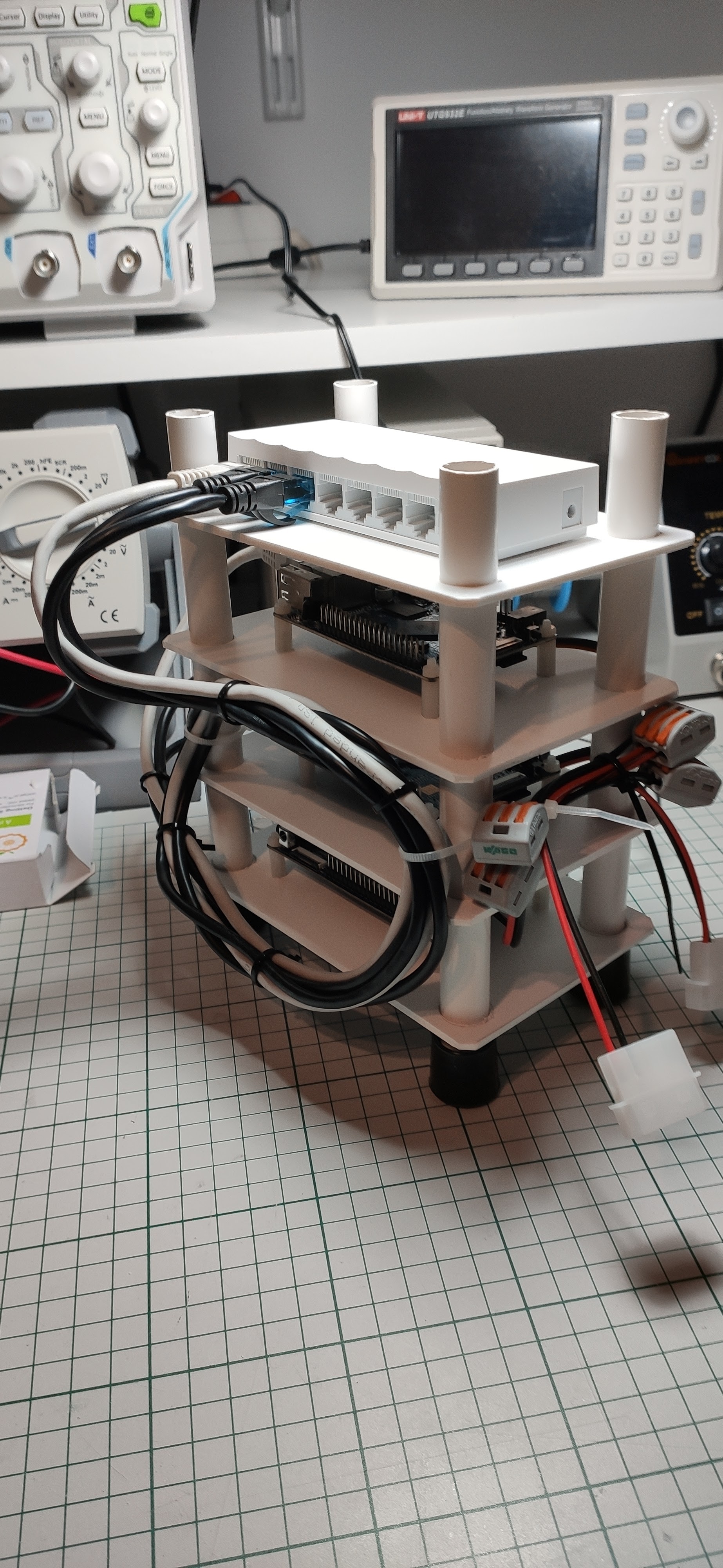
Next I sliced and prepared some sheets of plastic:
Made some bigger holes on each corner in order to push the pillars as you’ll see in a moment.
The four pillars of constitution
Had some white plastic tube laying around so I sliced it a little bit… Then I went further and pieced together all the floors of the main building.
I will let the images again to speak for themselves:
Cable management? Yes, please ! Well not that much cables to manage but still why not tie everything up so that we can avoid a “hairy” situation.
Networking
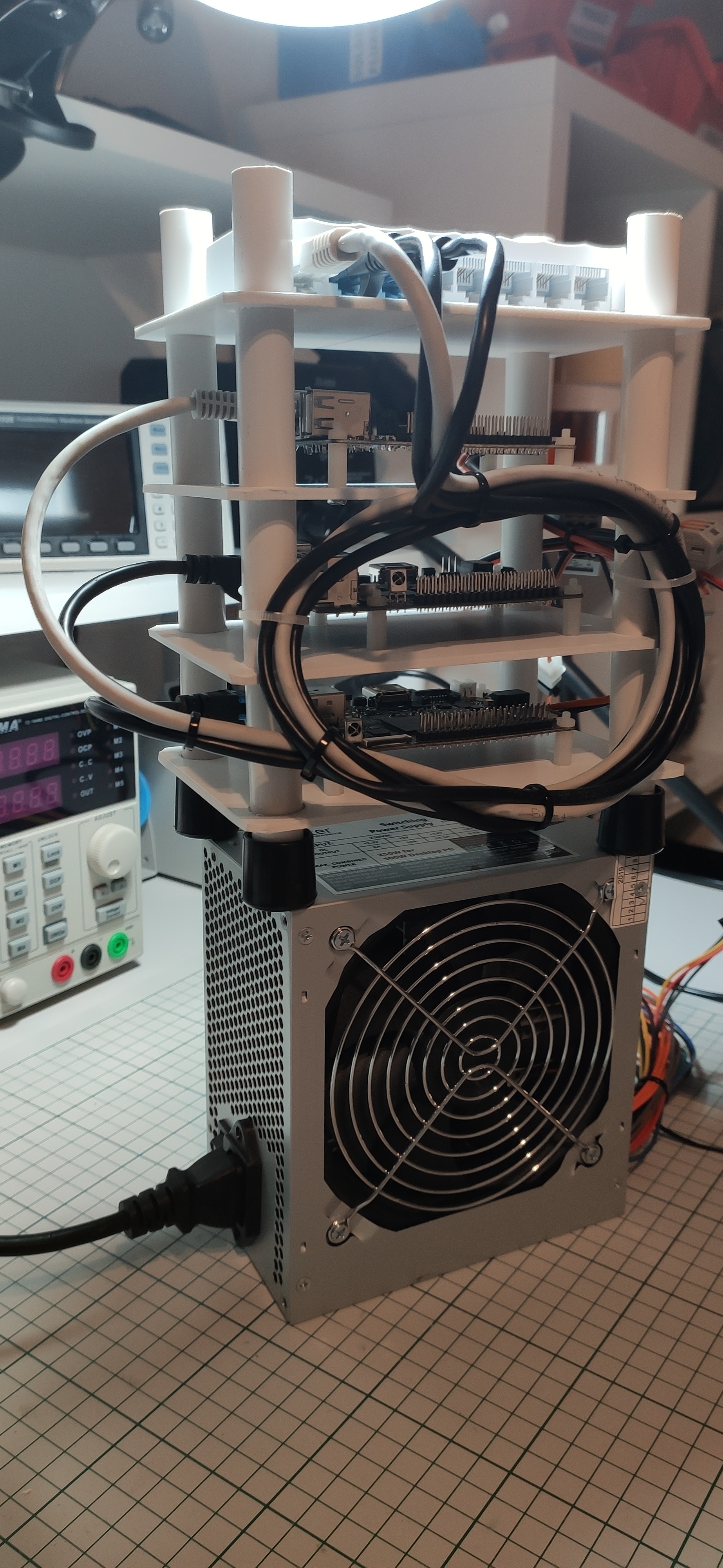
Not much to say only that at the top of the building is the almighty network switch as you can see in the above picture . It’s a cheap TP-Link8 port switch which works quite well for this project I would say.
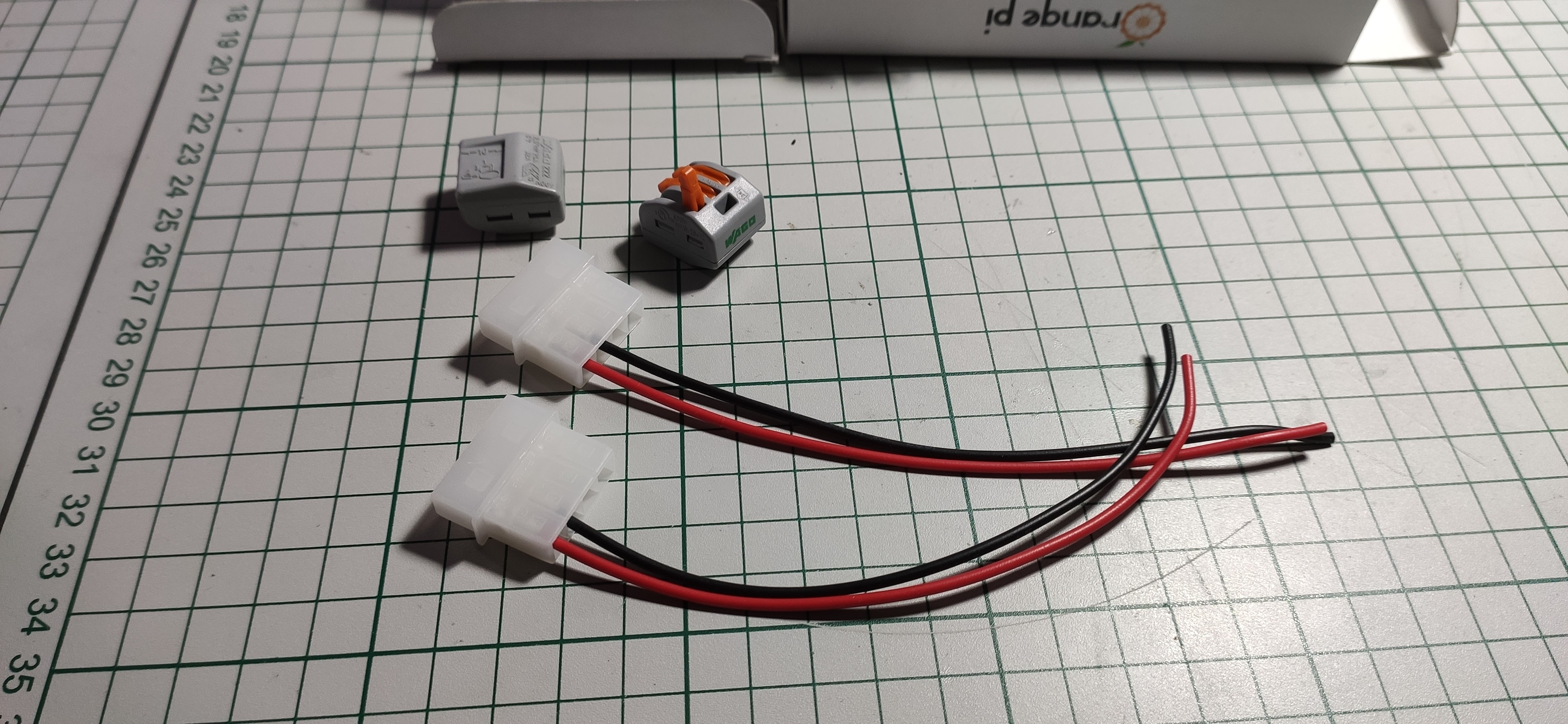
Powering the project
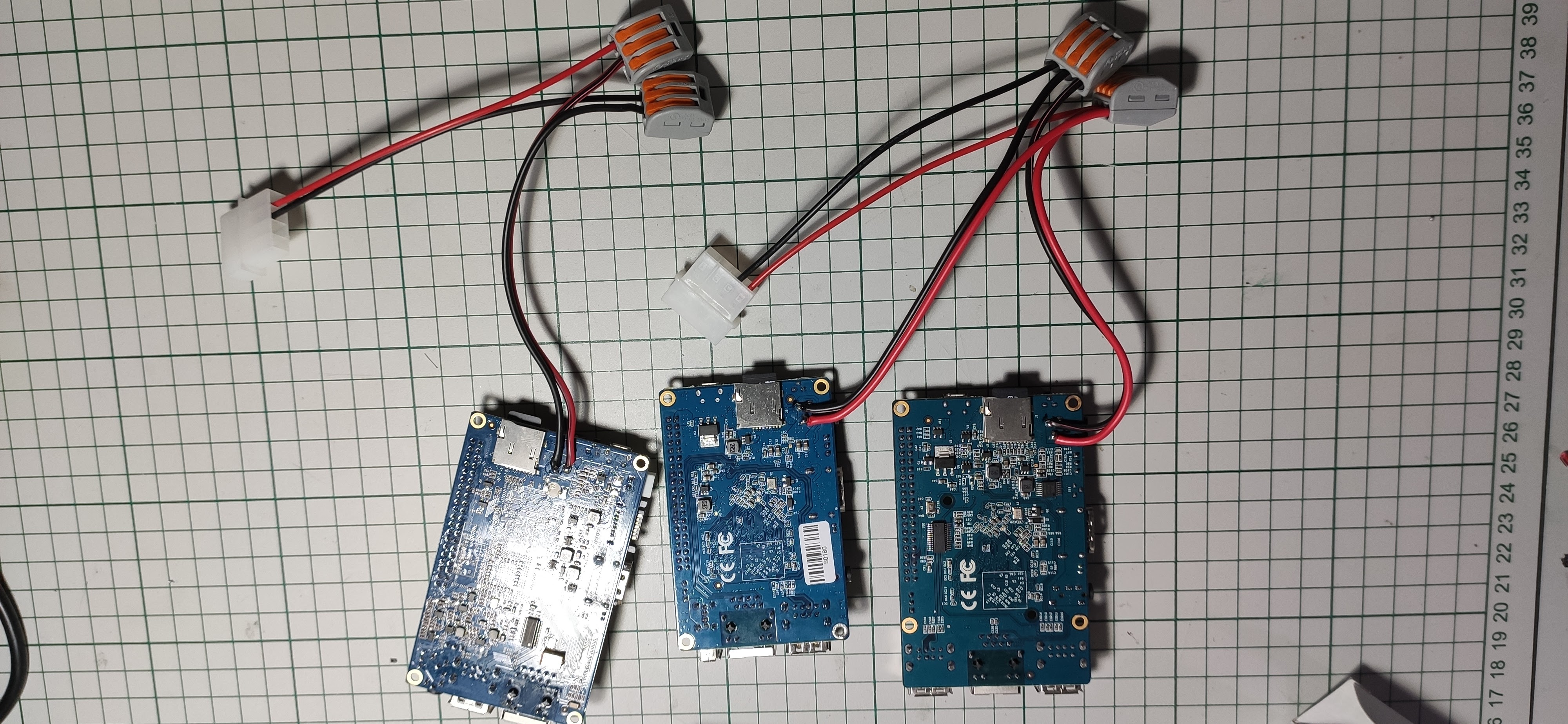
Easily achieved via a PC power supply using only the 5V rail. One board requires around 10-15W of power if I remember well so we need a power supply able to provide 3 x 15W = 45W which should be fine (I took the worst case scenario into consideration). The PC power supply that I’m using is able to provide that level of power and even more for future upgrades so we’re all good on this part. I will do some power consumption measurements at some point in time as well to see exactly the numbers but for now let’s go with some empirical thinking. I used two MOLEX connectors in this build so that we can better distribute the power via the cables. Here I’m talking more about balancing the current via two paths rather than one – more copper the better right? And for simplicity and ease of disassembly later on if required I think that some WAGO connectors really come in handy.
Conclusion
Overall I am pretty happy with the hardware build. We have now a small “tower” of compute units ready to go but who knows maybe it will reach the clouds one day and turn into cloud computing right ?
In my previous post I talked about the front plate of this project and now it’s time to talk a little bit about the power horse that makes this thing kicking and alive.
As in every electronics project design the most overlooked part is its power supply. What people need to understand that this is the most important part and must be taken care of with high priority. The performance and stability of the whole project depends on the quality of its power supply design.
Main design and concepts
Getting back to our project I have to say that this is a special power supply design that haunted me for about 2-3 years. It took so long because… well I had other stuff also so I was bouncing back and forth trying to make this work.
Finally I stumbled across this application design note from Power Integrations called DER-622. It’s a really great company offering really good products and lots of examples for creating power converters. They also have a online designer that will create everything for you: the final schematic, PCB and BOM. It’s called PI Expert – very powerful. Before finding this good resource I had a few ideas but none of them were let’s say good enough to power the final design.
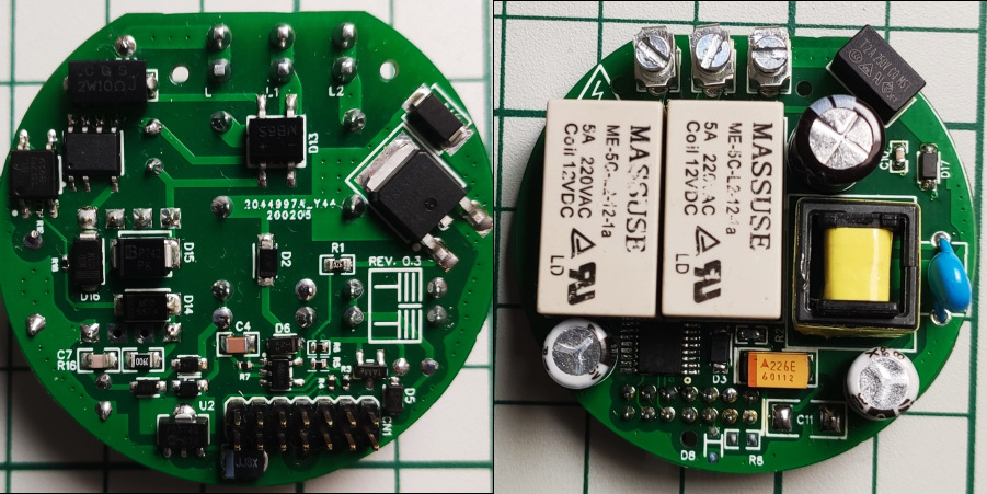
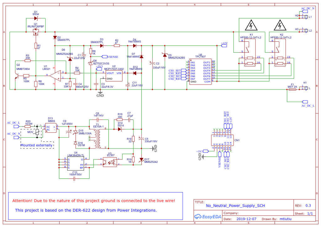
So based on the DER-622 application note I came up with my own custom design with a few modifications. Here’s the final schematic:
I didn’t reinvented the wheel here so it’s basically the original design but having the stand-by power supply changed so that it uses the now ubiquitous LNK364 IC delivered by Power Integrations of course. Also some components like the main MOSFET, LDO regulator and some diodes were replaced with equivalent ones which could be sourced more easily. The main driver for the latching relays was replaced also (in the original design some Darlington transistor pairs were used). I had to shrink this design as much as possible so that it could fit in the box from the wall.
How the power supply works?
As you can see from the schematic diagram it has two parts:
a standard AC/DC converter referred to as the stand-by power supply
a series regulator block built around the MOSFET and the opamp comparator
The stand-by power supply
This is not something new it’s just a standard AC/DC converter built around the LNK364 solution from Power Integrations. The EE10-A1 transformer was very easy to find on AliExpress and luckily it was in good shape as many products from there can be – you know – fake ones, desoldered from other products, etc so in another words: lack of quality control.
It’s my first design of this kind as I used only already made AC/DC converters like the HLK-PM01 just to give you an example. But I learned even more in the process by doing this kind of stuff so – success.
Most of the AC/DC converters are built using a flybacktopology and work on the very same basic principle:
a startup circuit built inside the chip helps the main oscillator to kick in and it gets powered via the input rectifier and filtering capacitor as soon as the input voltage has a sufficient value
the main oscillator drives the main MOSFETon and off via a feedbackloop built around that resistor divider from the output of the power supply, the Zennerdiode and the optocoupler
the MOSFET will drive the primarycoil of the transformer when it’s ON so that it will store magnetic energy which then gets released in the secondary coil when in the OFF state
the feedback circuit will modulate the oscillator so that it changes the on/off duty cycle of the MOSFET leading to a stable output voltage set by the Zenner diode (which in our case is set to 12V)
What’s nice also about this topology is the fact that the user is isolated from the mains via that transformer. This also helps to share a common ground for both the standby power supply and the series voltage regulator block of which I will talk about in a moment.
The series regulator block
And now things start to get more interesting . The main function of this block is to provide energy to our front plate when the main switch is turned on.
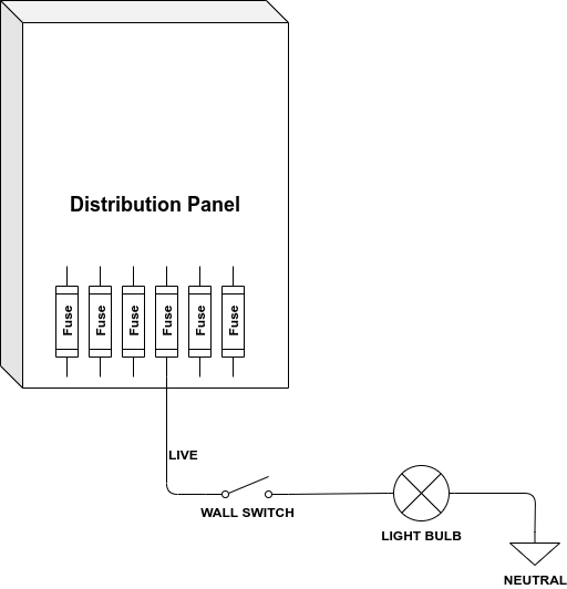
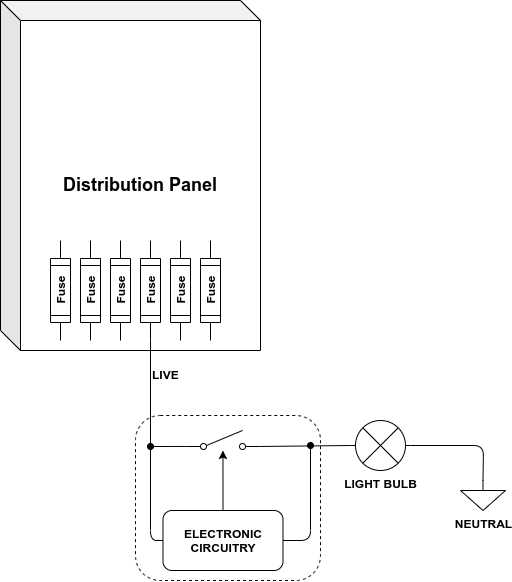
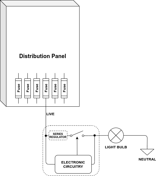
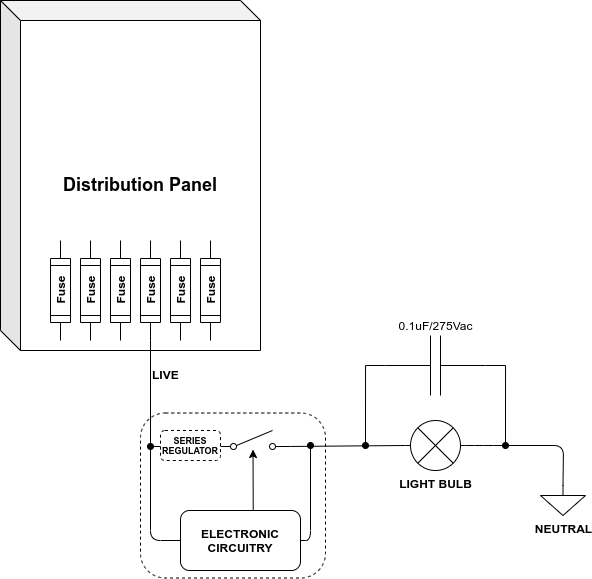
Why do we need this complexity? Well if you remember from the part one of this series of posts we need to power everything by only using the live wire from the wall. I will put another diagram here for better visibility.
So we want to get from this:
to this:
Seems simple right? We have our electronics that need to be powered in parallel with the switch and it should be able to get power like that. When the switch is open all the voltage is present on the switch so our stand-by power supply will be powered just fine but the current passing in this series configuration will and can be limited by the light bulb. But remember we need power and power is composed of: V x I which means both voltage and current will contribute. So even if the current is limited by the light bulb we should be able to take power if the voltage is high enough right? And this is true to some extent because the mains voltage is pretty high (we’ll talk a little bit more about this later).
But still something is wrong here – can you spot it quickly? OK let me do that for you by responding with another question: what happens when the switch is closed? The answer is pretty simple – it will short our circuit rendering it unusable!
And because of that situation we need something like:
What changed is the addition of a series regulator circuit along with the switch and that’s the block built around that MOSFET from the main schematic of this design. The main purpose of that series regulator block is to provide power to our electronics when the switch is closed. From the DER-622 application note this is how it works:
Since Q1 is in series with the line, it must handle the load current, which can be as high as 2 A. The op-amp U1 circuit block controls Q1 switching to allow low-power dissipation by fully turning ON the MOSFET once the threshold set by D6 (12V) + 3.3 V is exceeded. The ON duration is set to about 10 ms by tuning the R-C circuit R7 and C4, tuning C1, and using hysteresis on the input comprised of Q2, R3, R5, R6, and R4. Diode D1 is added to prevent the load current from passing through Q1 body diode once the MOSFET turns OFF.
This design has several drawbacks also:
latching relays have mechanical elements that can decay over time
they make noise when switching on and off (not very noticeable, but still …)
they are more expensive than a traditional relay and sometimes hard to find because of being not so popular
Safety?
Another important aspect of a power supply design is its safety of course and especially when working with high voltages. The input is protected for overcurrent via the 2A slow blow fuse (F1) and for high voltage spikes there’s that varistor or MOV that can be mounted externally (due to space constraints on the PCB). The inrush current is limited by the 10ohm resistor (R20) rated at 2W.
The PCB traces were made as wide as possible where needed in order to handle medium-high currents (<=2A) and also doubled on both sides. I also used the “via stitching” technique in order to reduce the capacitance and maybe help a little bit with the thermal dissipation. Because we’re working with high voltages also (around 230Vac and 310Vdc) I tried to stick to a minimum of 2-3mm between traces although a 5mm would be desired but yet again due to space constraints it was a little bit hard for me to accomplish that.
The PCB design
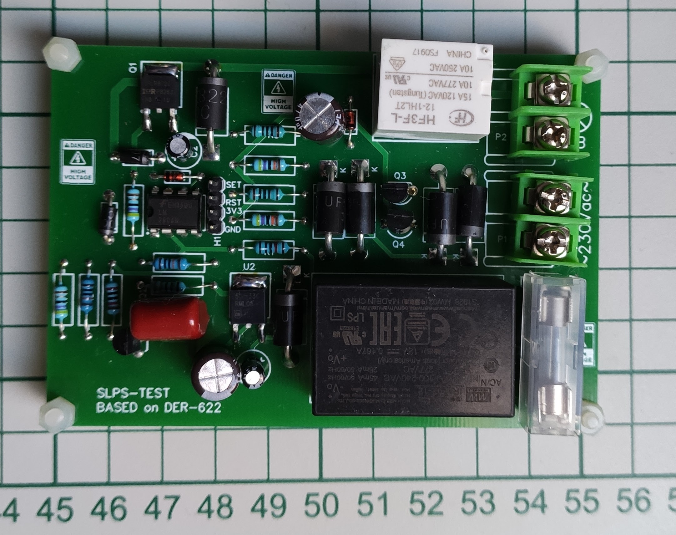
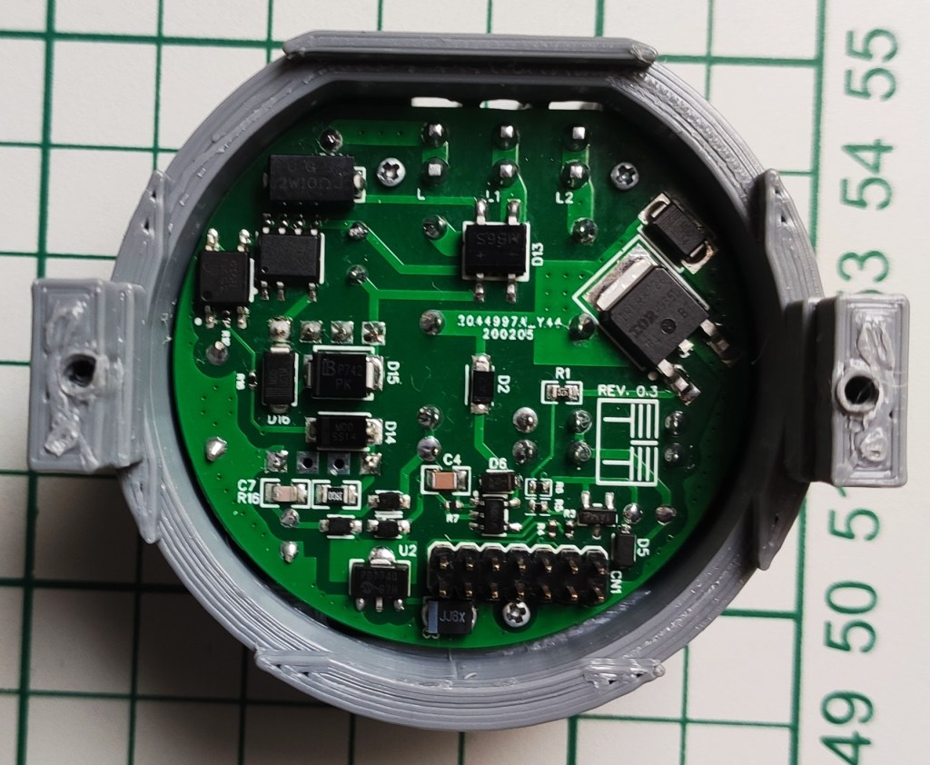
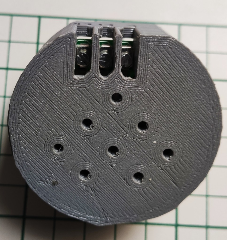
Initially I made a test board but not on a breadboard and it looks like this:
This was just to test and validate that this design really works on my side also and it did. So I was then happily moving to the next phase of the design and get done with the final thing which started to look like this:
And yes it borrows the dimensions and more or less the layout of the original Livolo board as I needed to make it fit in the wall and also be compatible with the front plate.
Overall I was extremely happy with this design and especially with the stuff that I also learned by doing it which is much more valuable.
Limitations
Yes there are limitations for this design as nothing is perfect.
One is the fact that this power supply gets its juice via the light bulb so in some cases (if not the most) the bulb will flicker when the switch is turned OFF.
Why?
Because being in series it draws the current via the light bulb and in some cases it may be enough to determine the internal power supply of the light bulb to start working but it won’t be able to do it fully so it will oscillate causing the flickering.
The solution?
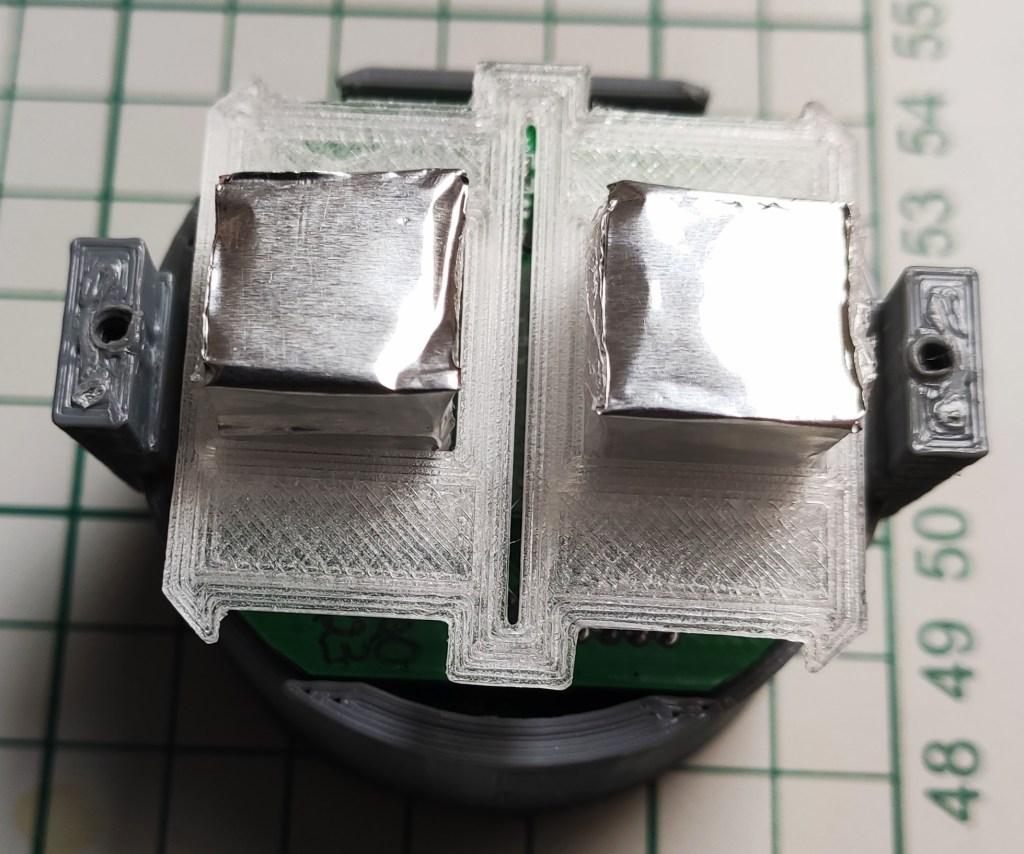
A bypass capacitor can be mounted across the light bulb. A 0.1 – 0.47uF / 275Vac capacitor will help to avoid the flickering.
The capacitor is not that big in size so it should fit in every light appliance from the wall or ceiling.
Other important things to consider:
If the power supply will oscillate or restart sometimes when switching back and forth in the ON/OFF states then the MCP1703 LDO output capacitor must be increased – I settled to a B casetantalum capacitor and a 220uF/6.3V value but maybe it will work with a 100uF/6.3V value also. This happens because when the board will switch from the stand-by power supply to the series regulator circuit and vice-versa there must be enough energy stored in the main capacitors: C2, C3 and C5 so that the latchingrelays get enough power to do their transitioning in a 20ms interval (this is set by the relay manufacturer and can be found in the datasheet as the minimumpulselength to trigger the relay). We also need power for the front plate during this time of course. And yes, the B case tantalumcapacitor will fit in the existing footprint from the PCB.
The inrush current limiting resistor (R20) was a little bigger than I expected so the footprint on the PCB was smaller but it can be soldered over one pad and then the other pin can be soldered over one of the main fuse pins which it connects to.
The final design including schematic, Gerber files and BOM can be found on my GitHub page here.
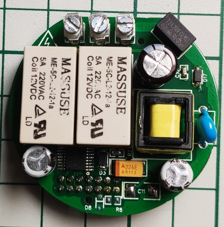
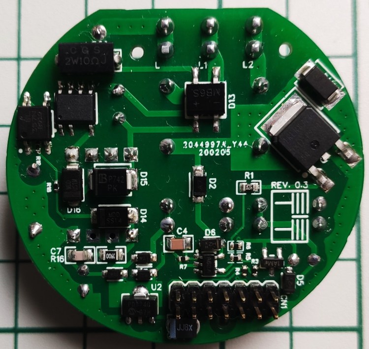
The final design and assembly
This is for the 2 channel variant (there’s also a 1 channel design):
In my previous post I talked a little bit about the switches I was working on and the required stuff in order to have a smooth integration with the existing infrastructure. And by infrastructure I mean the existing wiring present in the walls in the majority of the European countries.
What we’re after in the end? A light switch that works with no neutral wire and wireless communications. Also low power consumption is important – I’m sorry but no WiFi allowed!
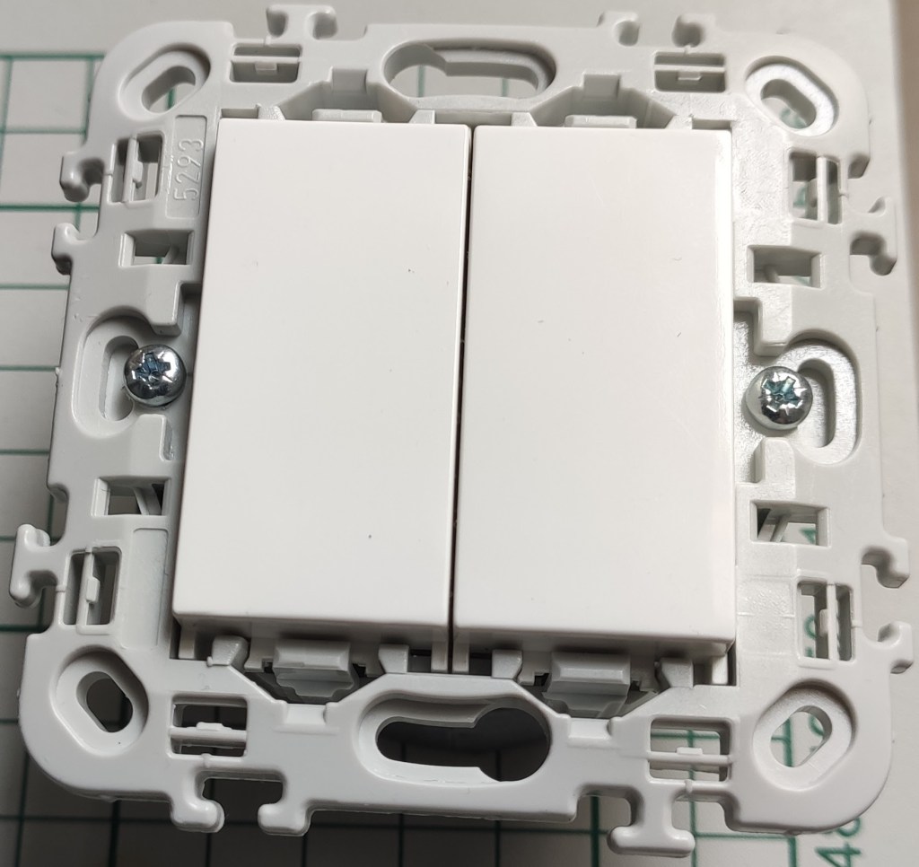
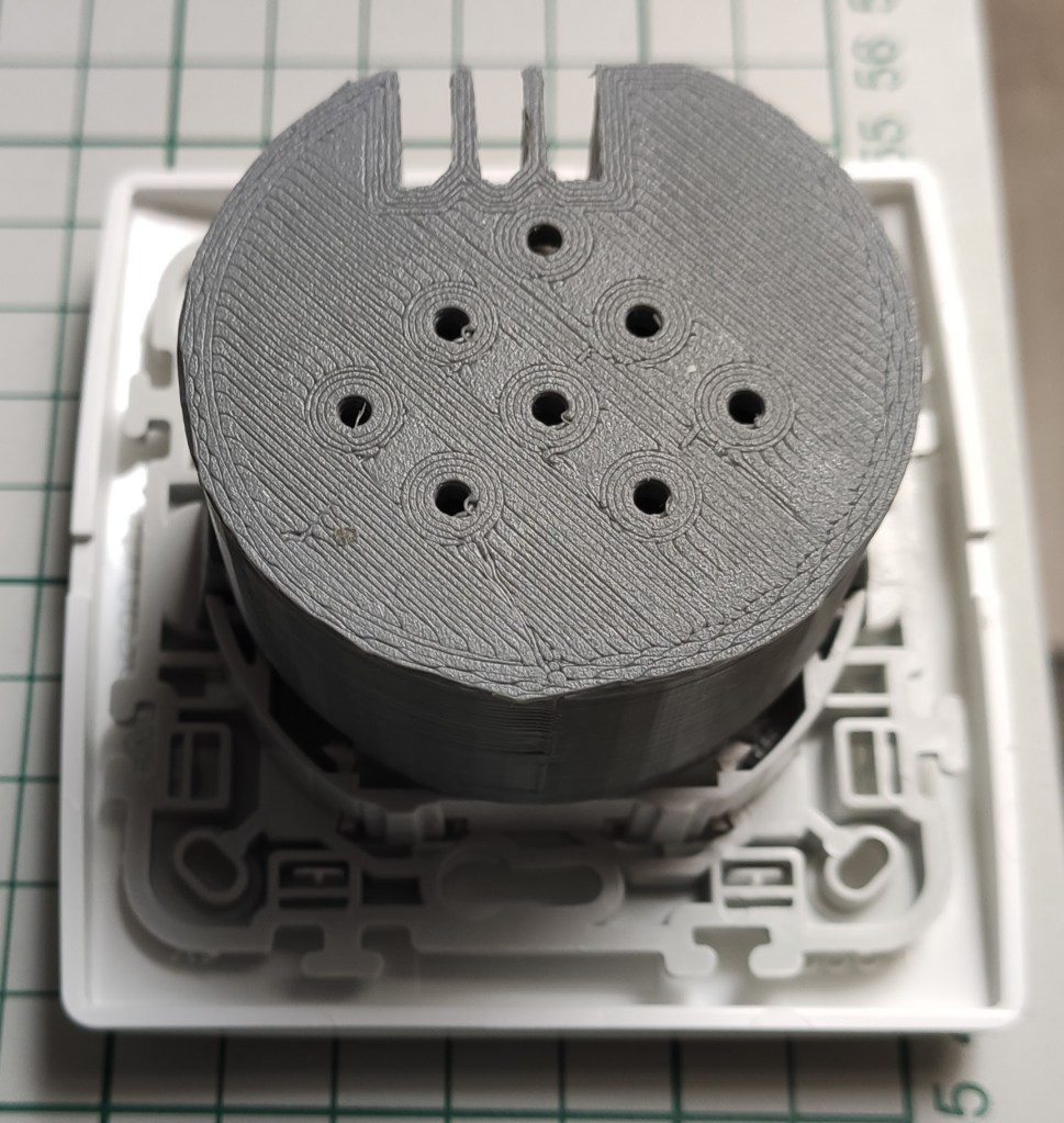
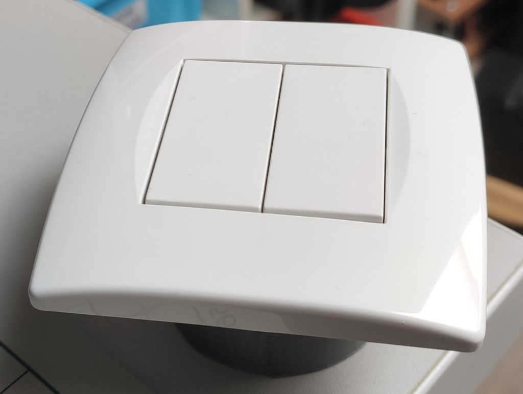
I also mentioned about the Livolo switches and you may ask why… well because it was the first switch that I came across and that accomplished most of my requirements. It’s a modular design also and the first easy thing to do was to replicate the front plate.
The original is on the left side and my replica on the right for comparison:
I wanted to do this because I needed a solution that fits in the wall and works only with the live wire. I also wanted to have wireless support of course.
And yes it worked but I wasn’t fully satisfied. Why? Because I had to buy an entire switch only to decommission the original front board and replace that with my replica. Of course it’s easier as you have all the parts in place and maybe cheaper.
But what if this switch will disappear one day or another hardware revision comes in and my replicated front board won’t fit again? This is not the only reason because I wanted to tune in the power supply also to my needs. And in the end why not have a full design for this piece of art and replicate the whole thing whenever needed. Make it also open hardware and give something back to the openhardware community. Let’s face it – this design is not something new and I didn’t invented it and most of the inspiration and knowledge that I gained from building it comes from the opensource community and/or articles published from various people/companies on the internet.
Continuing the above I have to mention about Power Integrations that helped/inspired me in building the so wanted power supply by studying their DER-622 publicly available document. And guess what? The power supply from the Livolo switches follows more or less the same design.
Other project that inspired me is the MySensors one and its great community – a lot of good folks in there with lots of knowledge.
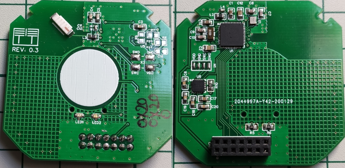
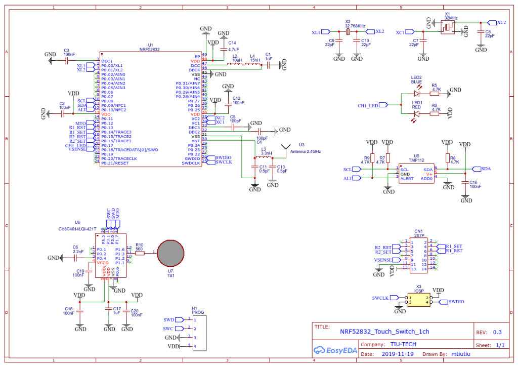
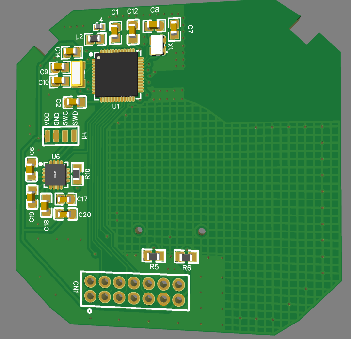
OK let’s discuss now about each module from this switch.
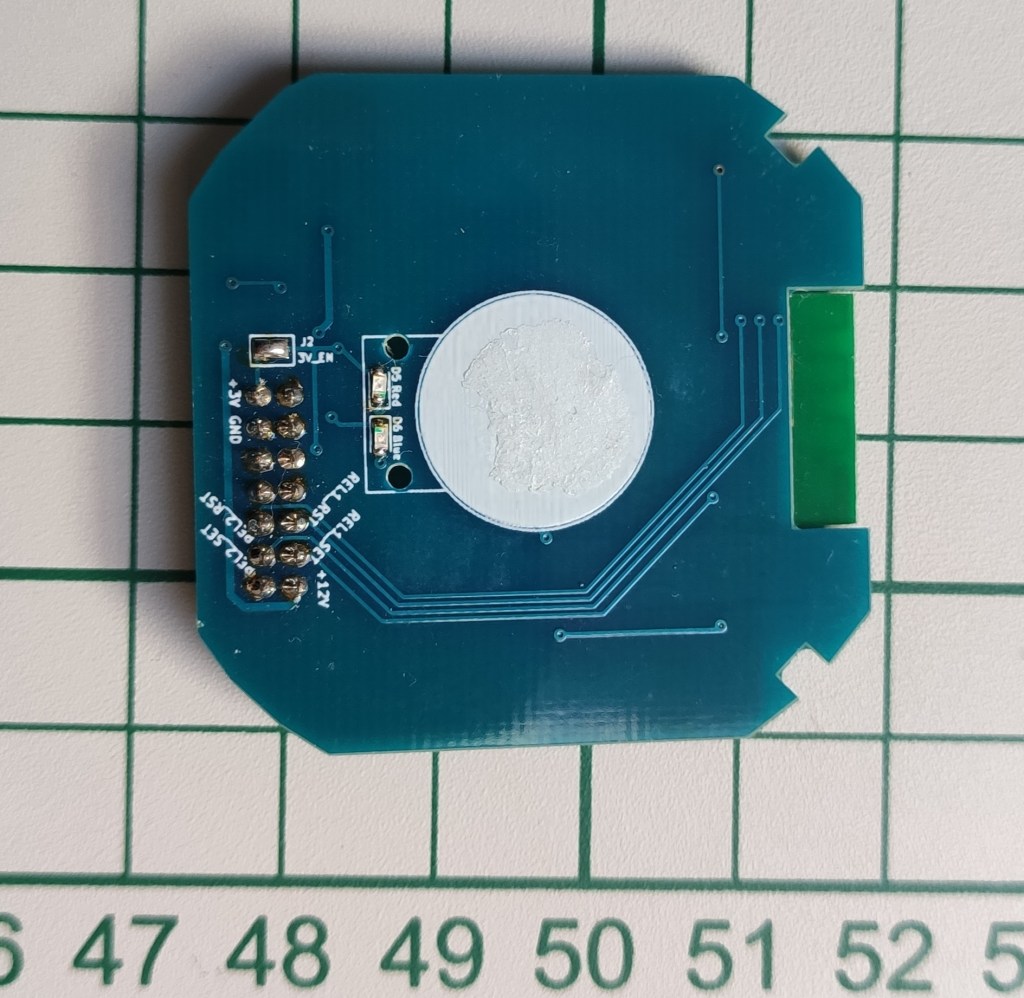
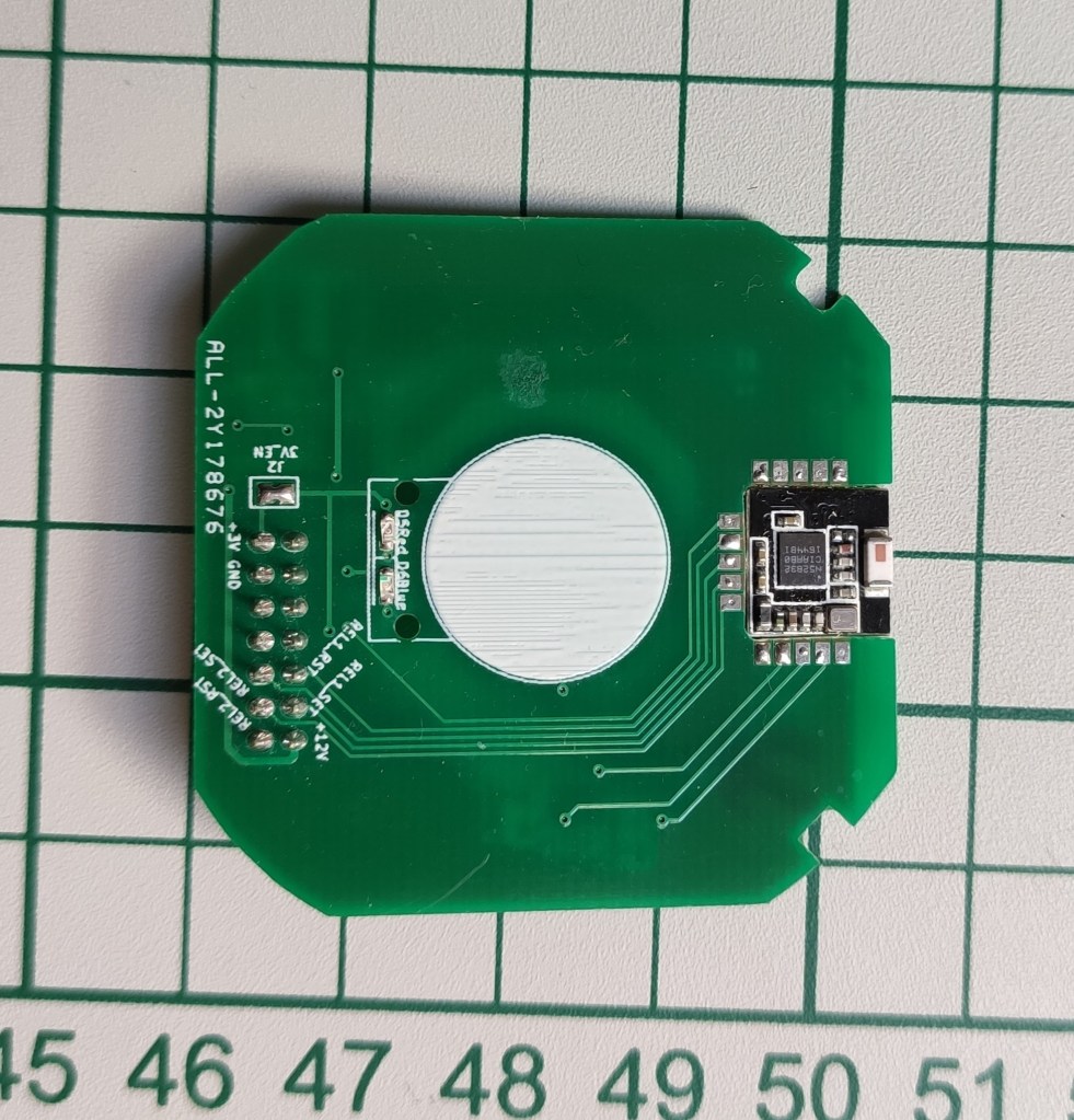
Touch sensing/control module
This is the front board which the user interacts with via that stylish and glossy panel. It has a MCU on it with touch sensing support. Now I’m not going to explain here how capacitive sensing works as there’s plenty of documentation about that on the internet.
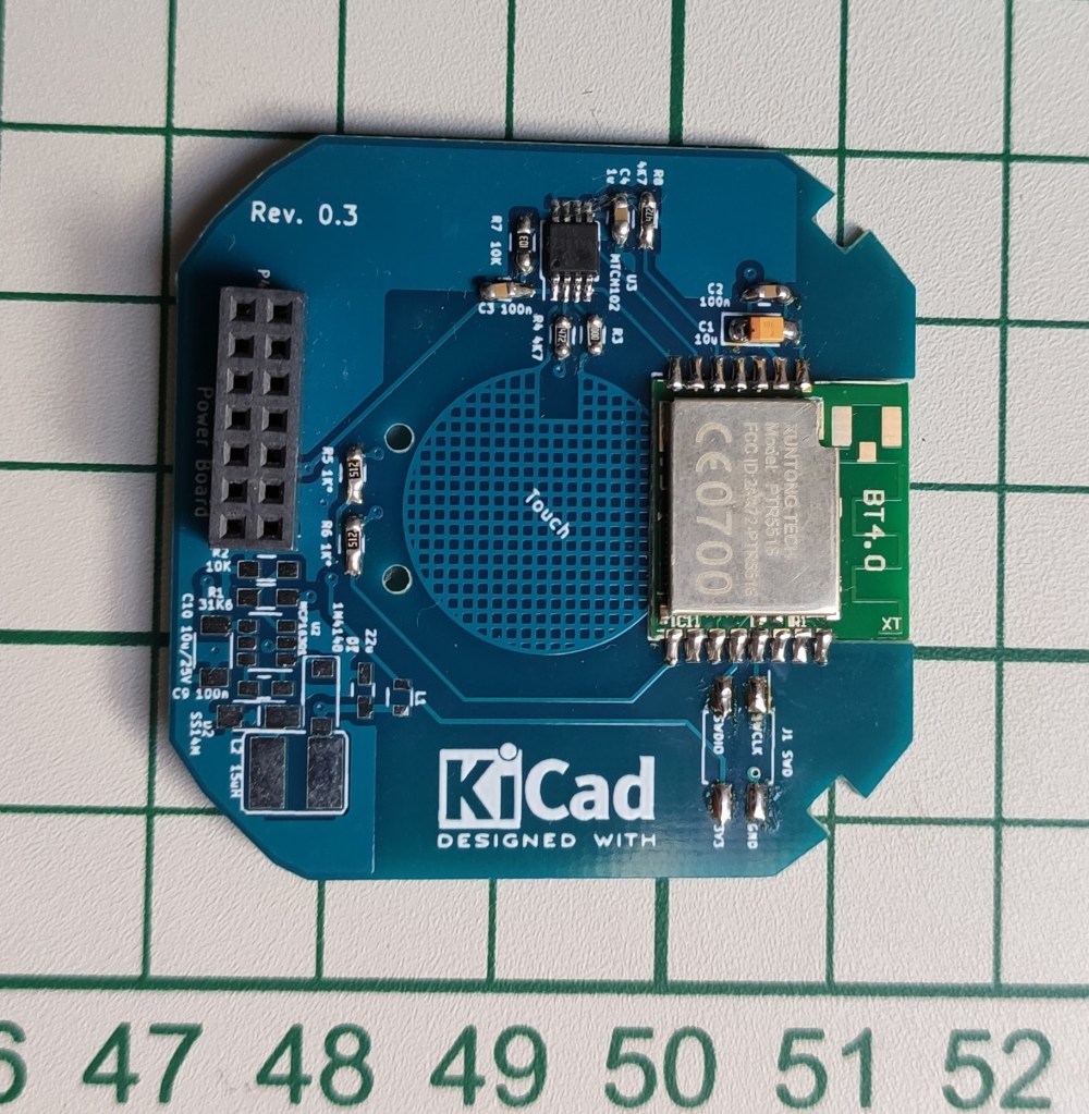
In my replica I added the well known RF SOC with Bluetooth support from NordicSemiconductor and more specifically I used the NRF51/NRF52 series. I picked this one as it has the best support when it comes to firmware, compilers, etc. and it’s pretty cheap nowadays also.
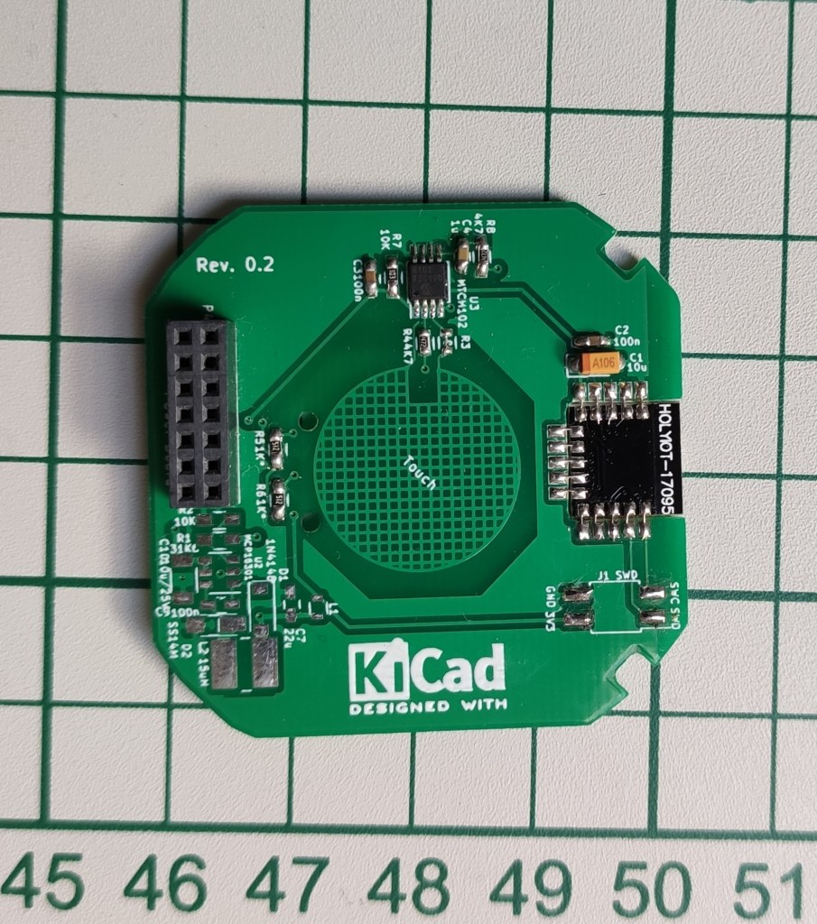
Initially I used some ready made NRF5xxxx modules bought from AliExpress like PTR5518, HolyIOT. For touch sensing I used the MicrochipMTCH10x capsense solutions which worked great also. Everything can be found on my GitHub page.
As I already mentioned in the previous post my first attempt for the radio/networking part was the MySensors project and the NRF24L01/RFM69 radio modules but with not so great success. I’m not saying that the MySensors project is not great or that it was because of it… I think it was a fault in my hardware designs and especially on the RF part which is kinda new for me when doing custom PCBs.
Yet again I wanted to learn and do more by going a little bit further and make my own variant so in the end this is the result:
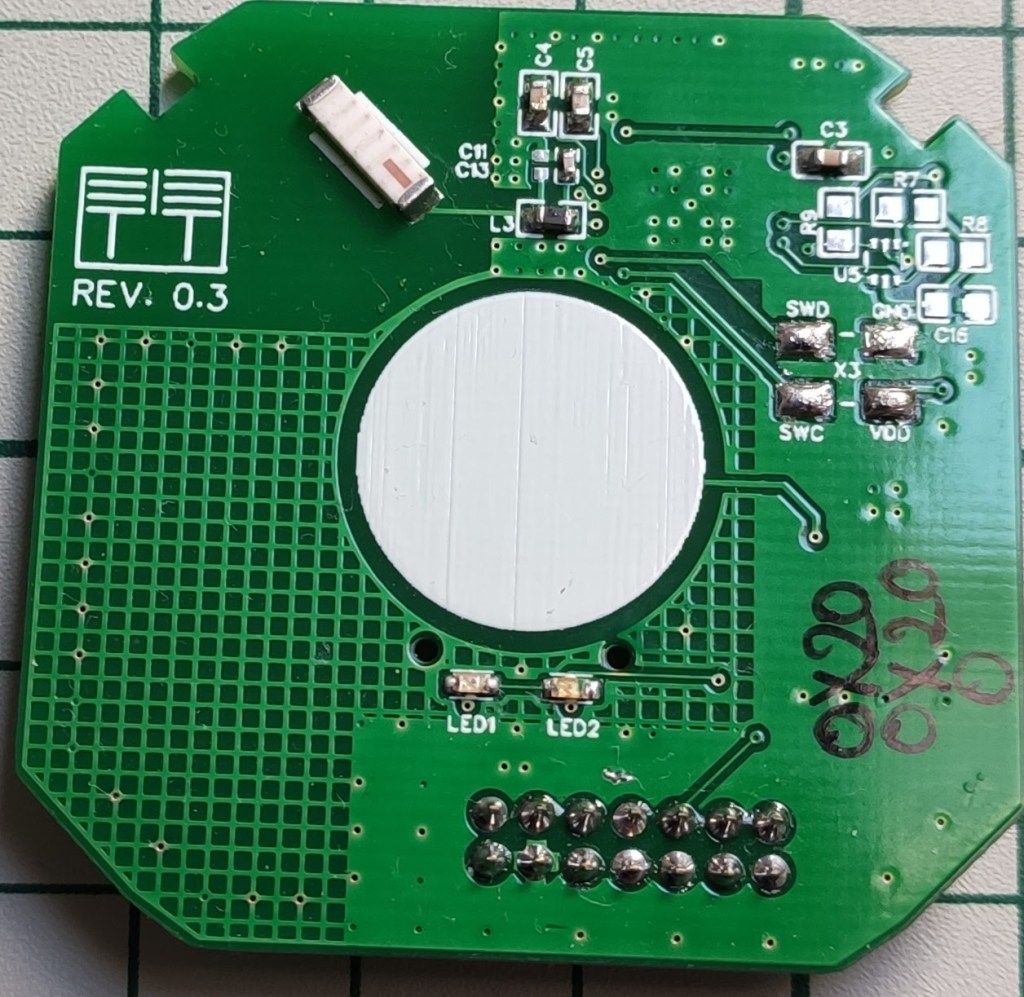
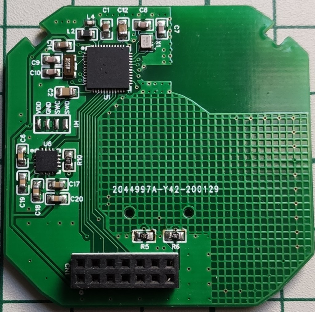
It’s a fully customized design now and we don’t need to rely on other vendors to buy their RF modules. Yes it implies more work but the final results are very satisfying. I also changed the touch sensing solution with Cypress Semiconductor ICs which are much better in my opinion. The final project can be found here (I didn’t mentioned but there’s also the two channel variant on my GitHub repository).
Ok so what we have so far is a custom module that has the following embedded:
Touchsensing support (provided by the CY8C4014 chip)
RF SOC powered by the NRF52832 chip – I ended using this one as has BluetoothMesh support also (more on that later)
Everything was designed using EasyEDA initially because I really love their ecosystem where you have everything in place starting from design to manufacturing and assembly – very powerful. I’m also a big fan of KiCAD of course but there are some things that I really miss in there compared to EasyEDA.
Schematics:
The heart of this hardware design is of course the NRF52832 chip from this great company called Nordic Semiconductor. They really have good solutions for building RF stuff (and no, I’m not an affiliate or doing promotions for them).
It’s a standard design based more or less on their recommended layout and application note(s). Of course this is my first RF custom design so it’s not perfect in regards to PCB layout and such but I tried my best to stick to the rules.
Next I used the wonderful IC’s of Cypress Semiconductor for touch sensing which in my opinion are best in class for this stuff. If you never heard of Cypress Semiconductor and of their PSOC solutions I do recommend you to do so – very powerful stuff (MCU and FPGA on the same die and a very powerful free IDE for doing the design).
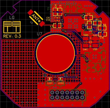
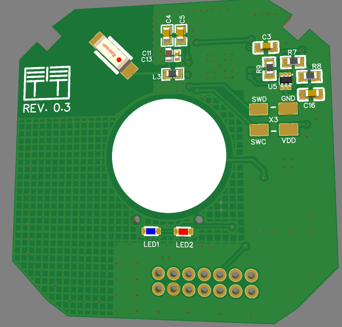
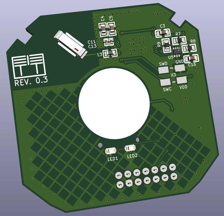
Front/Bottom side of the PCBlayout:
Some 3D renderings of the board:
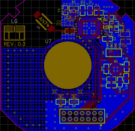
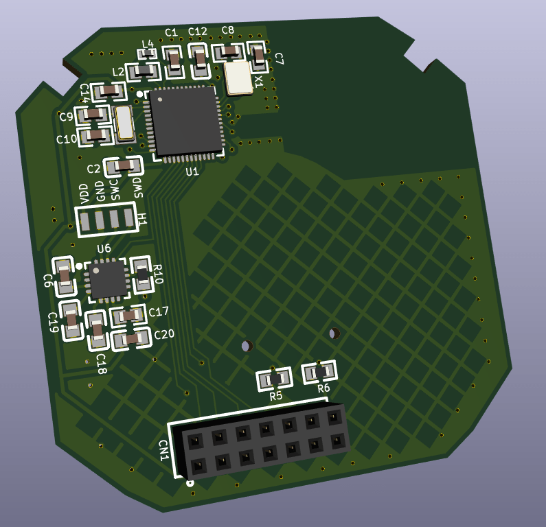
I also ported this design to KiCAD (PCB only) using this very cool utility called easyeda2kicad.
Just for you to see how this project looks in KiCAD – Godlike!
This is where KiCAD shines and it also offers other powerful features like STEPexport for doing MCAD and 3D printing custom plastic enclosures (which I did for this project also).
Software
There’s a long story for the software side also going from using the Arduino/MySensors core and dedicated Bluetooth libraries to ApacheMyNewt and ZephyrRTOS.
I won’t go into details here but what I settled on is the ApacheMyNewt and BluetoothMesh support that it offers.
Why ApacheMyNewt and not Zephyr?
Well I won’t go into a debate here as both are very great projects and production ready I would say but I liked the simplicity and the build system from the ApacheMyNewt project. Also its YAML structured projects and the way you define a new BSP (Board Support Package) is very powerful. It’s much easier IMHO and not very messy compared with the Zephyr one where you use that menuconfig based system and oh my… so many options and dependencies to choose from. This reminds me of the days when I had to recompile Linux kernels from source code and the associated headaches. The Zephyr project is backed by the Linux Foundation and trust me it really has great support and lots of features and supported boards packed in. So it’s not a throw away thing at all but I don’t very like its build system – although now it seems to be supported by Platformio which balances things a little bit.
The final point to touch is the Bluetooth Mesh support that this custom board has now and trust me this is such a cool thing.
Bluetooth Mesh networking as any other mesh networking technology is a very powerful thing/concept and packed with lots of features. Some of the most important are in my opinion:
Extended range/coverage
High availability
Security from the start – this is not quite a characteristic of a mesh network but it should be part of it as it’s so important nowadays
Of course the internals are pretty complex and not fully yet understood by me yet but I can say that from a application development perspective I have enough knowledge to make it work and do something useful. It’s very important to understand and grasp its concepts first and then look over the code and examples. Otherwise it’s very painful and frustrating but once you get the idea everything starts to come along nicely and things get more clear.
Bluetooth mesh builds over the existing Bluetooth protocol adding some extra layers and features like (just a few to name):
Server/Client models (and many other models as everything here is thought as a “model” – you’ll hear a lot about that)
Publish/Subscribe pattern – this is so powerful also
Repeater nodes
Low power nodes
Friend nodes that work in conjunction with low power nodes that are battery powered and cannot stay ON all the time
Another nice thing that I also like is the fact that you can use the phone to provision the network and configure it how you want without reflashing the firmware on the nodes. Even more – you don’t need a gateway (this is only needed if you want to face the internet or other networks using another protocols) or a coordinator or other special nodes to keep the mesh network running or to have extended functionality. It’s so independent and working on its own even if a node or more fails it will still work! (well assuming that you have other nodes in range to replace it otherwise the coverage will be affected but the network functionality will not suffer from it)
The final code that I made for the light switches can be found here. For the Cypress Capsense part the source code can be found here. This is a separate project as it gets deployed onto another MCU and it’s made using the PSOC Creator IDE from Cypress Semiconductor (which was now acquired by Infineon).
In order to understand it you need first to grasp the Apache MyNewt projects structure, OS concepts and the Bluetooth Mesh side. There are plenty examples on their GitHub repository also.
The above source code was tested (it’s in “production” now) and works without a glitch on the already deployed light switch nodes in my house.
Let’s not forget – one does not need to use the final custom board that I made because this is the beauty of having a modular design. We can easily swap it with one of the other custom boards that I made or you can make your own as long as the hardware interface (that 2×7 pin connector) respects the standards from my schematics. What may change is the MCU GPIO pin assignments and that’s all.
Flashing the firmware
It’s all documented here but let’s tackle it a little bit also in this post. The whole project source code is based on the ApacheMyNewt project so it follows its standards (well more or less but I tried to stick to it as much as possible).
I divided the source code files (and headers) based on the sub modules that the hardware part has like:
Touch sensing logic
LEDs logic
Relays (actuators) logic
Mesh logic
The touch sensinglogic has to deal with reading the capacitive touch sensor signals and act accordingly on the actuators or the relays. It also deals with debouncing.
The LEDs logic is pretty simple and self explanatory – it only triggers the leds.
The relays logic deals with triggering the latching relays by creating the necessary pulses and it also keeps relays or better to say light channels state in memory (like which channel is in the ON or OFF state). The thing is that the power supply board has a feedback mechanism in order to see in what state the system is when powering on as well. So I did this in a simple way by keeping state in some variable stored in RAM. It’s a simple approach and it works. Another important thing to mention is that the relays logic has a a dedicated safety mechanism created in software so that whenever there is a power outage it will always force the system in the OFF state when power comes in. This is needed because the relays used on the power supply board have memory so you don’t want the lights to turn ON on a power break and maybe you’re not home. This make also the system predictable as I will know that it will always start in the OFF state on a power cycle.
The mesh logic has to do with the networking stuff and it’s the biggest part but not that big as the Apache Nimble project took care of most of the details for us in the background. The source code structure is pretty standard and I just adapted one of their examples to my needs. So before trying to understand the code I strongly recommend to study the Bluetooth mesh primer from the Bluetooth SIG website. It’s very well documented there and not bloated with lots of not so useful explanations.
What we’re most interested in here is the handlers of messages which trigger these two functions in the code: gen_onoff_set_ack(…)/gen_onoff_set_unack(…) and gen_onoff_get(…).
The first one is called whenever there’s a new message addressed to us and containing the ON/OFF payload (which is a 1 or a 0) because we’re using a GenericOnOffServer model. The other one as the name implies is when a GenericOnOffClient requires us to give it our current ON/OFF state. And yes as I mentioned in this post somewhere we do have a client/server architecture in this mesh networking system which must be familiar to you.
The other stuff in the source code deals with defining the required models that this light switch node has to offer and the Bluetooth subsystems initialization, etc.
Building the project
Apache MyNewt has a pretty cool build system and ways of organizing/structuring the source code by following a well defined pattern. I do recommend reading the concepts first in order to accommodate.
Let’s build now the source code for the 1 channel custom board that I made. Here are the required steps using a Linux shell terminal (can be flashed from a Windows command prompt or PowerShell also):
Bootloader (this is the same for any channel variant). The following lines are flashing and loading the bootloader on the custom board:
For flashing the board one needs a standard CMSIS-DAP programmer – I’m using a stlinkv2 clone reflashed for CMSIS-DAP compatibility. The interface is a standard SWD one so nothing special here (any CMSIS-DAP adapter can be used even a standard st-link clone which I think requires some modifications).
Provisioning/Configuring the mesh network
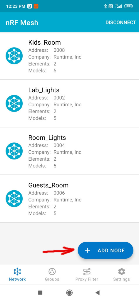
First we need the Android app (there should be an IOS version also). It’s important to leave one node to act as a Proxy at a minimum. This is the default state also when a new node is flashed for the first time.
Initially the network is not formed as we don’t have any nodes provisioned at all so the first thing to do is to “Add” a new node by using the big blue button from the main application screen.
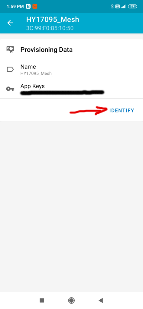
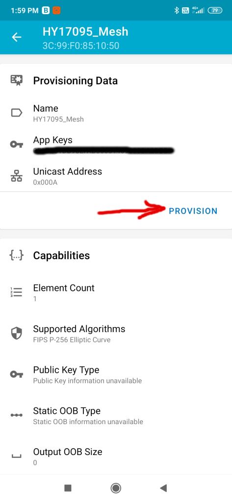
The unprovisioned node should appear then in the next screen. We click on it and then hit “Identify” and “Provision“. The whole process should not take more than 10s or so. You can also edit the node name afterwards – this is not relevant for the process or for the app it matters only for us the humans to know what purpose it has.
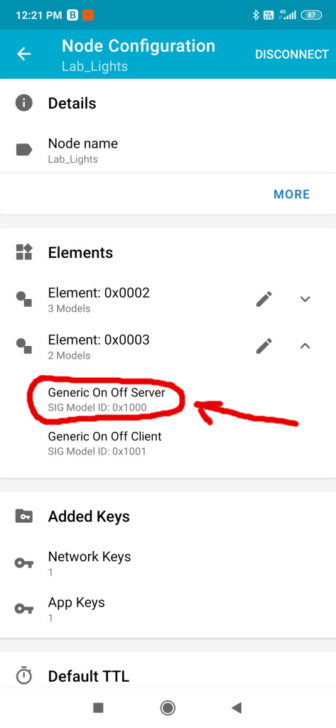
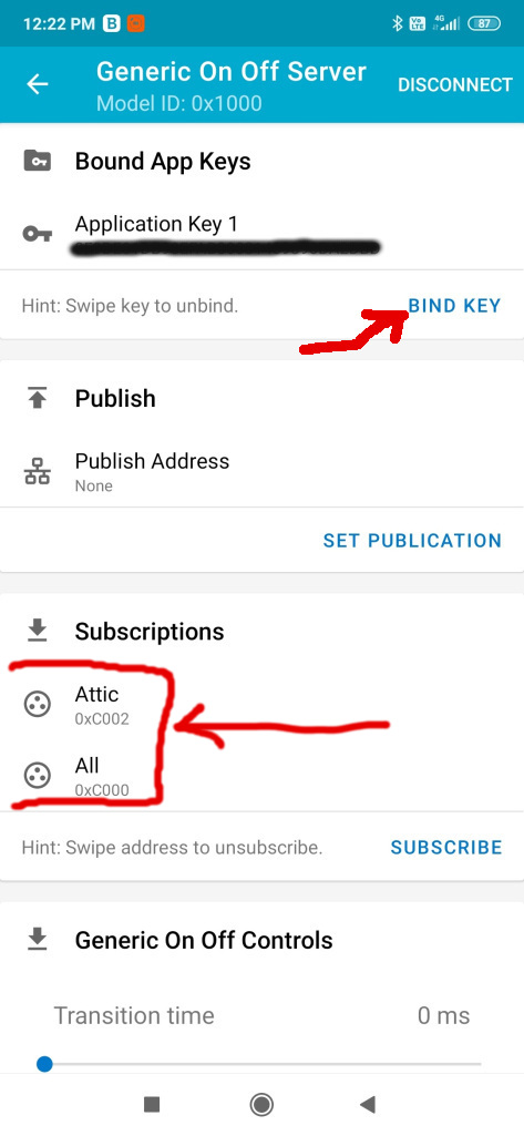
Next we need to configure the Generic OnOff server (this represents basically the light that we want to change its state to be either on or off) and bind an application key to it. Yes everything is secured in a Bluetooth Mesh network. There are separate keys used to encrypt and identify traffic both at the network level and the application level. So please be very careful not to share the keys or make them visible. You can also configure subscriptions here – in may case I created to groups beforehand (can be done from the application also). I can subscribe to more than one group and receive commands from both. In my case I have a specific group for where the lights are located and the other one is “All” so that I can act on all at once if I want to.
Then in the groups screen you can play with the lights and turn them on or off based on the associated group – trust me this is so cool! Then when I leave my house I can set an automation to turn everything off for example. Or I can set another light switch which is near my main entrance to act on the “All” group and turn off all the lights like that. I can do this by subscribing its Generic OnOff Client to publish to the “All” group – isn’t that cool? Oh and all the settings that you do when configuring the network are persistent (using the MCU internal flash memory).
The next step after configuring the network is to back up the settings from the application by exporting them somewhere safe. This is an important step to do after you configured the network because the application won’t retain those settings if you change the phone, reset it or uninstall it. Why is this needed? Because the topology of the network, node id’s, application and network keys, groups, etc are saved in a json file which it reads upon start. Sorry but we don’t have network discovery or stuff like that yet. The mesh network will work without this part or without the phone but you won’t be able to reach it via the proxy node(s) because you don’t know or have the keys, etc… so keep this important back up step in mind. You will be able to import or re-import it later if desired.
Another thing you can do is tune the network settings like the number of retransmits and interval for messages both at the network level and for nodes.
I didn’t mentioned but the Bluetooth Mesh uses internally a mechanism called managed flooding. This means that messages are not routed by a process which results in them being transmitted along a specific path comprising a sequence of only certain devices. Instead, all devices in range receive messages and those which are acting as relays, retransmit the message to all other devices in range. All packets include a field known as the TTL. This may be used to limit the number of hops that a message takes as it is relayed. Heartbeat messages, transmitted by devices at intervals, include information which allows the network to learn about its topology and the number of hops away, each of the other devices is. This allows devices to set TTL to an optimal value, which avoids messages being relayed an unnecessary number of times.
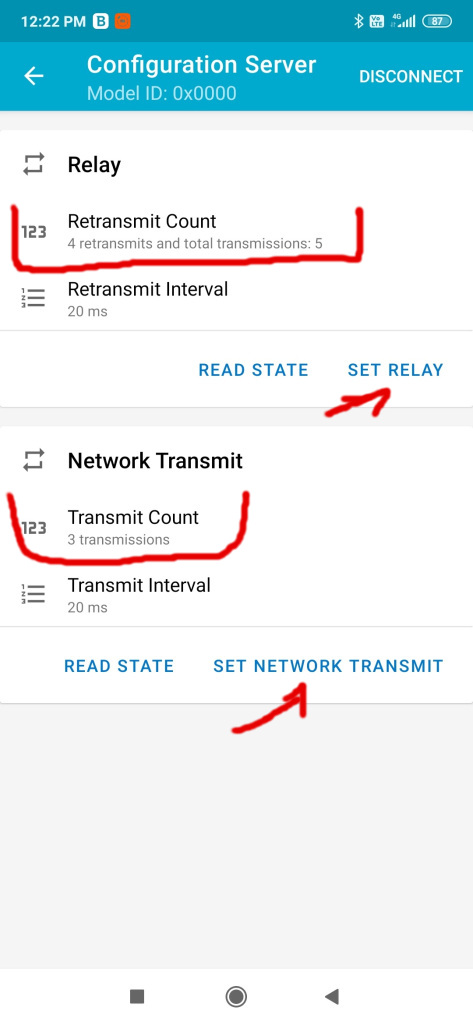
From the nrf mesh application one can tune the above mentioned stuff as seen here:
Basically you can tune the number of retransmits to suit your environment but don’t go very high as this increases the traffic and the collision rate of messages. This helps if the environment is a little bit noisy or if metallic obstacles are present in the walls, etc. I had to double in my case the number of retransmits from 2 to 4 and increase by 1 the network retransmits. But again as I said earlier this needs to be tuned for each environment. Oh and these settings are persisted on the nodes and it’s a per node setting. Other things to consider is the number of relaying nodes and where those are placed. In my case I configured all the nodes to perform relaying but it’s not necessary. You can disable relaying from the firmware at compile time or from the app as seen in the pictures above by pressing the SET RELAY button and configure the retransmits counter to 0.
Further documentation about the bluetooth mesh networking and lots of interesting stuff can be found on the official Bluetooth SIG page here and here which I do recommend reading as well as other articles on that subject present there.
Lots of things to discuss about this project and mesh networking but I think this will suffice for now.
In the next post I will be talking about the power supply design which was the most challenging part for me. Let’s not forget that this is the most important part of every electronics project in this world and also the most overlooked part! Do you agree with me?
At the beginning there was darkness lots of darkness until intelligent light switches appeared and suddenly things started to change and make people lives much more “brighter. OK enough storytelling … because I don’t believe this and neither do you.
A friend of mine asked me if I could automate his home lights so that he could switch the lights on and off at its will and in each room independently. I replied – why not? I like to automate stuff more than anything so this was an opportunity for me to put some things into practice. More than that I thought – pff, light bulbs ON, OFF, ON… that should be a piece of cake, right? Well… the reality turned to be a little bit different.
Requirements:
First and the most important one – we should integrate with the existinginfrastructure
Touch sensors
Radio control and feedback
Let’s take each of the above and discuss in detail:
Infrastructure: Here in the EU we have classic mechanical switches and a simple wiring in the walls as we don’t need more than that. So starting from the main panel from where all the “electricity” is distributed in the house we have this:
So how can one replace the above mechanical switch with an electronic one (with touch sensors, radio, bla, bla …) and keep the existing wiring/infrastructure? Well some of you might say it’s impossible – how to power up an electronic device using only the live wire and close the circuit via the light bulb back to neutral.
Making the impossible work ?
After some while of searching and doing research I found out that the magic works based on some preconditions:
Having two power supplies – yes two are needed: one for the OFF state (stand-by) and one for the ON state.
The electronic switch must drawverylittlecurrent in the OFFstate and this is achievable based on the fact that every light bulb has some leakagecurrent because of the electronics inside it (CFL or LED bulbs) and for the incandescent ones – the electricresistance of the filament. Basically we steal some energy this way in order for our custom circuit to be always powered.
In the ON state – this is the happy case because when the circuit is closed there’s enoughcurrent to make all work but there must be a low and sufficientvoltagedrop across our custom electronic switch so that it has again enoughpower to work.
First inspiration – Livolo ?
Let’s talk about the Livolo switch construction details a little bit. It has two boards inside it:
One for the power supply and relays
One for the touch sensing part and LED signaling
There’s a variant which has a radio receiver in it also – which is more expensive but it doesn’t provide feedback because it only has a radio receiver and not a transceiver so not good for us (things changed meanwhile and now they provide a ZigBee solution but not very cheap). What we can do about it? Well the first and obvious thing to do is to replicate the front board with a custom one which has touch sensing support and BLE in our case and make it work and behave according to our needs. Now we have so many options out there in choosing a radio solution and a microcontroller but not all of them are good for our project here.
Why ??? Well… because:
We need a MCU combined with a radio transceiver that draws very little current (ideally a few milliamps on average and even lower)
We need good software support and open source is a must
We need a low component count in order to reduce complexity, cost, maintenance, deal with space constraints …
What I tried and experimented so far:
A custom solution made by me using Arduino boards and custom software/radio protocol over radio transceivers low level libraries(I tried RFM12, NRF24L01, RFM69, and many others) – I gave up because it needed too much work for one man and it wasn’t very reliable (the software part and my custom protocol – which worked to some degree so hey it wasn’t too bad in the end because I learned some more stuff too)
Next there was ( and still is actually) the great MySensors project – this one worked very great for me to some degree but when it was put into practice along with Livolo switches and other actuators where high reliability is desired… well it was not doing so well in my case.
And the final step and last thing that I tried – BLE. In the end it turned out to be the most reliable way of making this switches work as expected and not crash so yeeyy! For this one I used the almighty NRF51822RF SOC chip from Nordic Semiconductor – thank you Nordic Semiconductor for creating this – it’s really a great chip. More than that it’s supported by the ARM GCC toolchain and by the Arduino community which is a big plus – oh my – dreams start to come true.
Some pictures of some custom front boards that I made using NRF5xxxx based modules from various vendors:
All the above modules work and have been tested with real Livolo switches. More details can be found on my GitHub projects page based on the module type and number of channels here.
In the next post I will describe in a little bit more detail the control board used in this project using a custom designed that I made. This is the final design on which I settled using the almighty NRF52832 chip.
I always liked to build stuff in general. Why? Because that’s what engineers or makers do. I think this is my very basic definition – a MAKER or a DIY guy.
It started a very long time ago when I was on the 8th grade and my father told me one day: why not try some other stuff like getting into electronics?
Well you may wonder why electronics? Because he noticed that I had some affinity for the only solid state receiver that we had around in the house which started to malfunction and I was very curious about it. At that time he showed me its schematic and when I looked at that green paper containing all those symbols … that’s where it all began.
Before throwing something to garbage why not try to make it useful again?
This was an interesting and also my first project of this kind when it comes to woodworking and yes I love making wood projects also.
This time wasn’t about creating something new but a let’s say “restoration” project. There’s this wood bench that everybody enjoyed in the neighborhood but sadly it turned into this:
So I was thinking why not give it a new life? And so it all started …
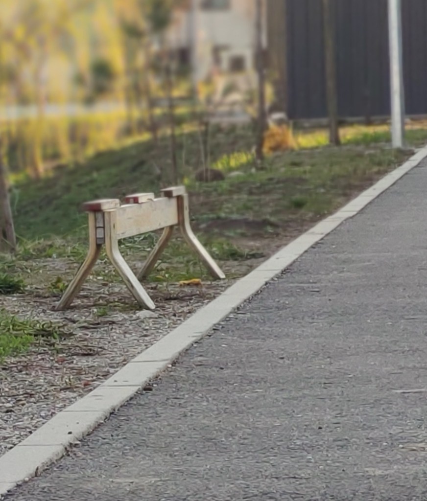
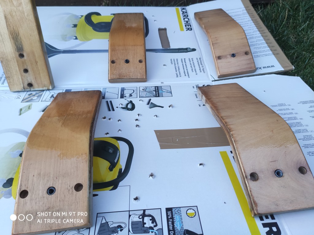
Legs disassembly and cleaning:
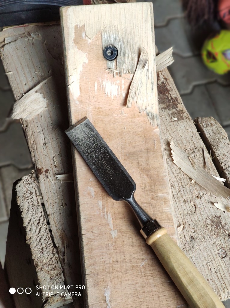
Next comes the central part which connects all the pieces together. After a bit of sanding and painting:
Legs cleaned and then painted:
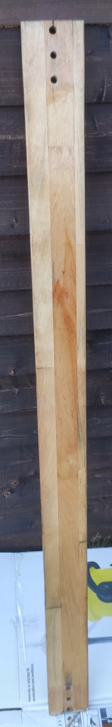
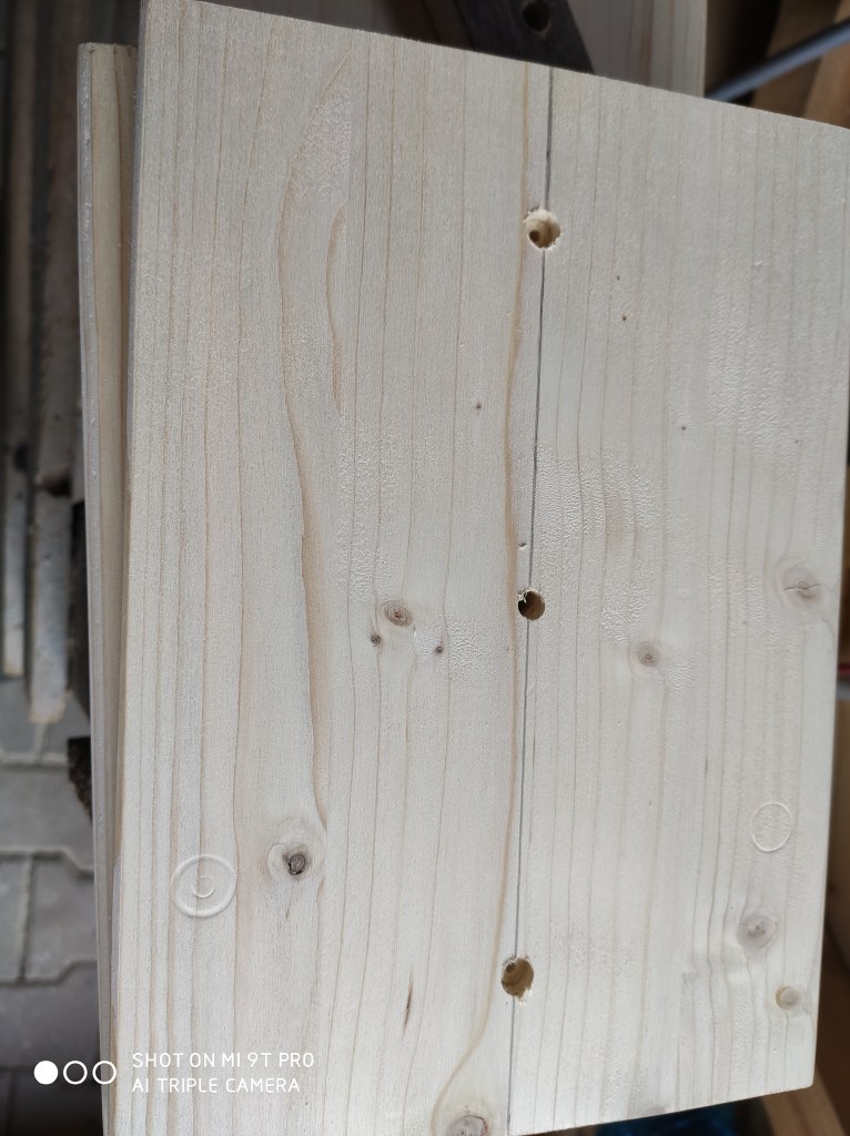
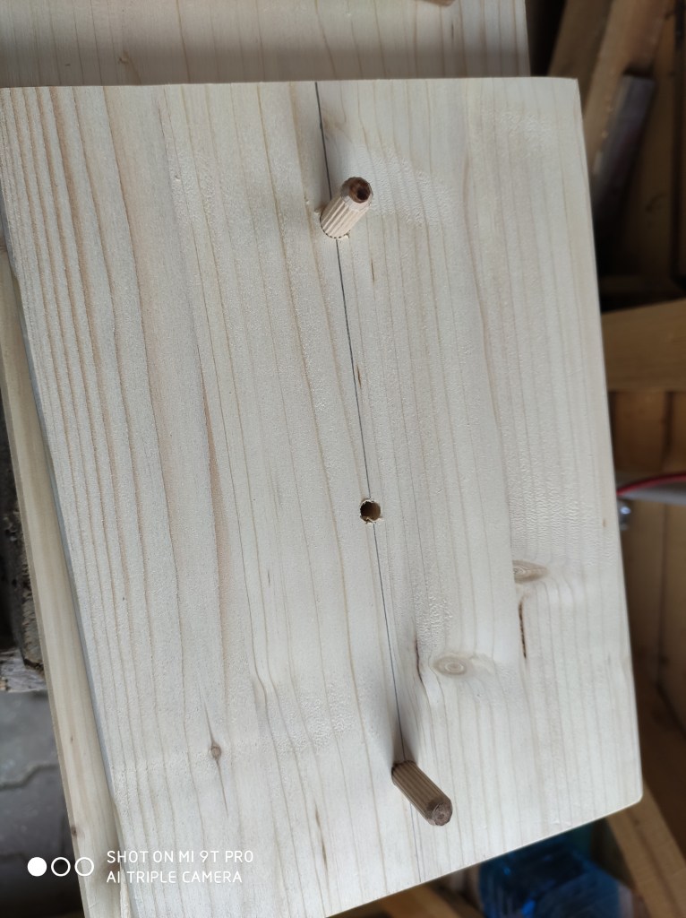
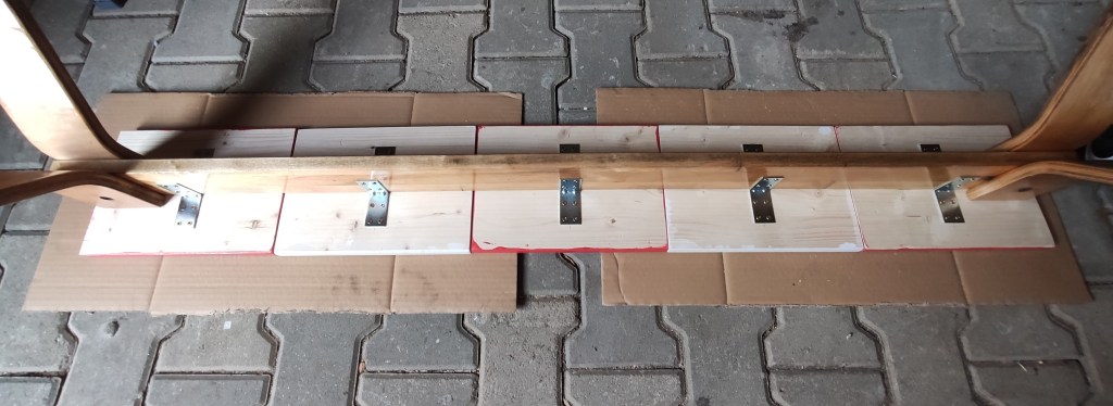
Now the wood plates on which you’ll get some rest after a long day of work …
Some reinforcements also:
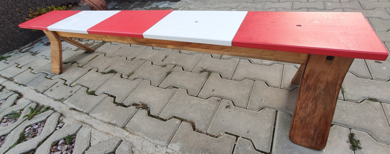
Finally the piece of resistance when all gets assembled and we get the final result we waited for after all that hard work: