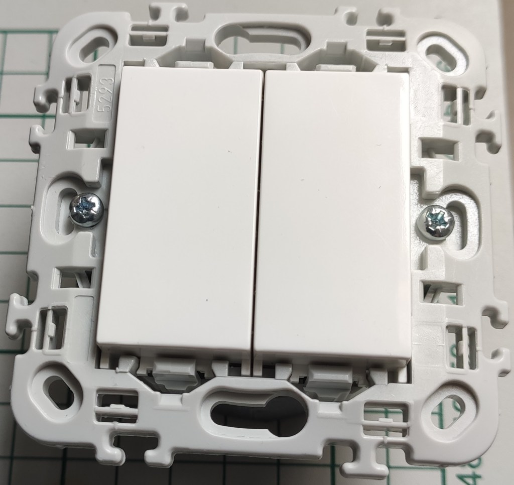
In my previous post I talked about the front plate of this project and now it’s time to talk a little bit about the power horse that makes this thing kicking and alive.
As in every electronics project design the most overlooked part is its power supply. What people need to understand that this is the most important part and must be taken care of with high priority. The performance and stability of the whole project depends on the quality of its power supply design.
Main design and concepts
Getting back to our project I have to say that this is a special power supply design that haunted me for about 2-3 years. It took so long because… well I had other stuff also so I was bouncing back and forth trying to make this work.
Finally I stumbled across this application design note from Power Integrations called DER-622. It’s a really great company offering really good products and lots of examples for creating power converters. They also have a online designer that will create everything for you: the final schematic, PCB and BOM. It’s called PI Expert – very powerful. Before finding this good resource I had a few ideas but none of them were let’s say good enough to power the final design.
So based on the DER-622 application note I came up with my own custom design with a few modifications. Here’s the final schematic:
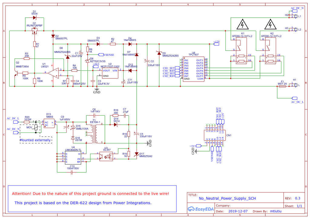
I didn’t reinvented the wheel here so it’s basically the original design but having the stand-by power supply changed so that it uses the now ubiquitous LNK364 IC delivered by Power Integrations of course. Also some components like the main MOSFET, LDO regulator and some diodes were replaced with equivalent ones which could be sourced more easily. The main driver for the latching relays was replaced also (in the original design some Darlington transistor pairs were used). I had to shrink this design as much as possible so that it could fit in the box from the wall.
How the power supply works?
As you can see from the schematic diagram it has two parts:
- a standard AC/DC converter referred to as the stand-by power supply
- a series regulator block built around the MOSFET and the opamp comparator
The stand-by power supply
This is not something new it’s just a standard AC/DC converter built around the LNK364 solution from Power Integrations. The EE10-A1 transformer was very easy to find on AliExpress and luckily it was in good shape as many products from there can be – you know – fake ones, desoldered from other products, etc so in another words: lack of quality control.
It’s my first design of this kind as I used only already made AC/DC converters like the HLK-PM01 just to give you an example. But I learned even more in the process by doing this kind of stuff so – success.
Most of the AC/DC converters are built using a flyback topology and work on the very same basic principle:
- a startup circuit built inside the chip helps the main oscillator to kick in and it gets powered via the input rectifier and filtering capacitor as soon as the input voltage has a sufficient value
- the main oscillator drives the main MOSFET on and off via a feedback loop built around that resistor divider from the output of the power supply, the Zenner diode and the optocoupler
- the MOSFET will drive the primary coil of the transformer when it’s ON so that it will store magnetic energy which then gets released in the secondary coil when in the OFF state
- the feedback circuit will modulate the oscillator so that it changes the on/off duty cycle of the MOSFET leading to a stable output voltage set by the Zenner diode (which in our case is set to 12V)
What’s nice also about this topology is the fact that the user is isolated from the mains via that transformer. This also helps to share a common ground for both the standby power supply and the series voltage regulator block of which I will talk about in a moment.
The series regulator block
And now things start to get more interesting . The main function of this block is to provide energy to our front plate when the main switch is turned on.
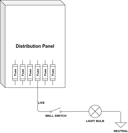
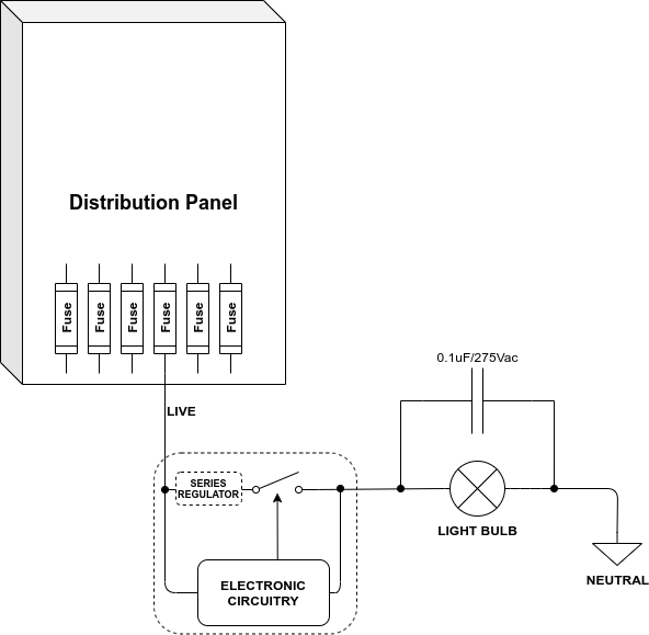
Why do we need this complexity? Well if you remember from the part one of this series of posts we need to power everything by only using the live wire from the wall. I will put another diagram here for better visibility.
So we want to get from this:
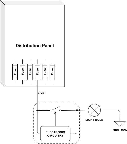
to this:
Seems simple right? We have our electronics that need to be powered in parallel with the switch and it should be able to get power like that. When the switch is open all the voltage is present on the switch so our stand-by power supply will be powered just fine but the current passing in this series configuration will and can be limited by the light bulb. But remember we need power and power is composed of: V x I which means both voltage and current will contribute. So even if the current is limited by the light bulb we should be able to take power if the voltage is high enough right? And this is true to some extent because the mains voltage is pretty high (we’ll talk a little bit more about this later).
But still something is wrong here – can you spot it quickly? OK let me do that for you by responding with another question: what happens when the switch is closed? The answer is pretty simple – it will short our circuit rendering it unusable!
And because of that situation we need something like:
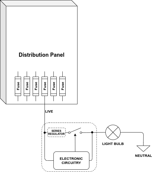
What changed is the addition of a series regulator circuit along with the switch and that’s the block built around that MOSFET from the main schematic of this design. The main purpose of that series regulator block is to provide power to our electronics when the switch is closed. From the DER-622 application note this is how it works:
Since Q1 is in series with the line, it must handle the load current, which can be as high as 2 A. The op-amp U1 circuit block controls Q1 switching to allow low-power dissipation by fully turning ON the MOSFET once the threshold set by D6 (12V) + 3.3 V is exceeded. The ON duration is set to about 10 ms by tuning the R-C circuit R7 and C4, tuning C1, and using hysteresis on the input comprised of Q2, R3, R5, R6, and R4. Diode D1 is added to prevent the load current from passing through Q1 body diode once the MOSFET turns OFF.
This design has several drawbacks also:
- latching relays have mechanical elements that can decay over time
- they make noise when switching on and off (not very noticeable, but still …)
- they are more expensive than a traditional relay and sometimes hard to find because of being not so popular
Safety?
Another important aspect of a power supply design is its safety of course and especially when working with high voltages. The input is protected for overcurrent via the 2A slow blow fuse (F1) and for high voltage spikes there’s that varistor or MOV that can be mounted externally (due to space constraints on the PCB). The inrush current is limited by the 10ohm resistor (R20) rated at 2W.
The PCB traces were made as wide as possible where needed in order to handle medium-high currents (<=2A) and also doubled on both sides. I also used the “via stitching” technique in order to reduce the capacitance and maybe help a little bit with the thermal dissipation. Because we’re working with high voltages also (around 230Vac and 310Vdc) I tried to stick to a minimum of 2-3mm between traces although a 5mm would be desired but yet again due to space constraints it was a little bit hard for me to accomplish that.
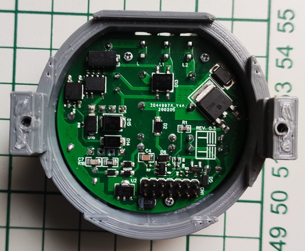
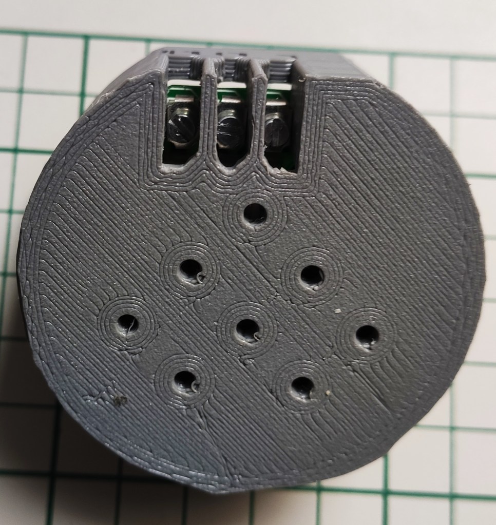
The PCB design
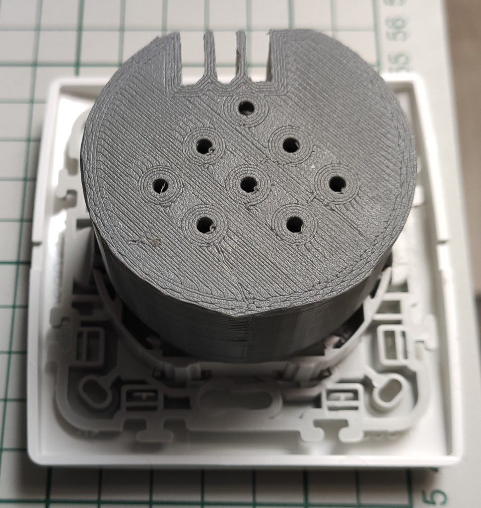
Initially I made a test board but not on a breadboard and it looks like this:
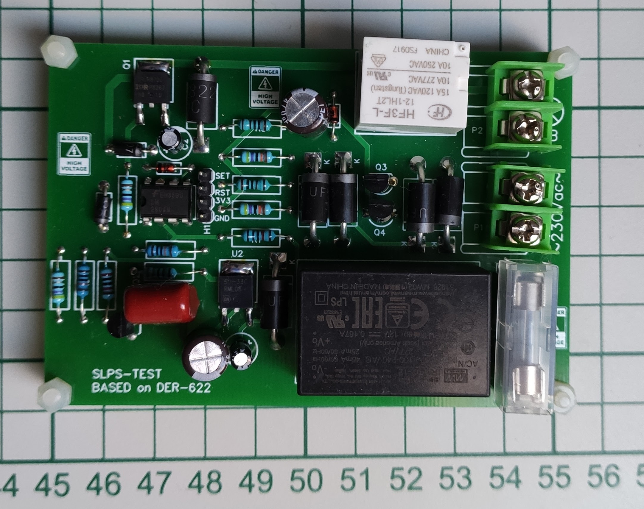
This was just to test and validate that this design really works on my side also and it did. So I was then happily moving to the next phase of the design and get done with the final thing which started to look like this:
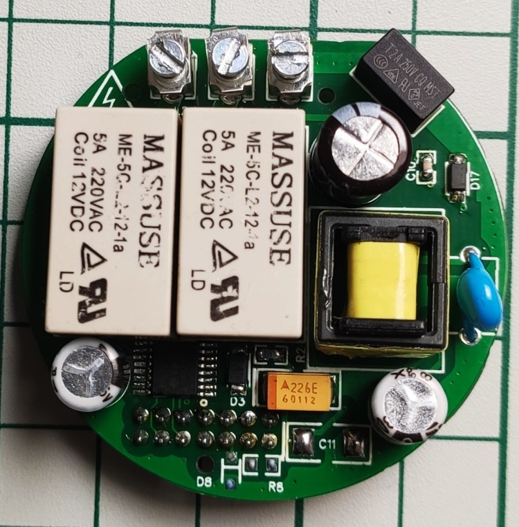
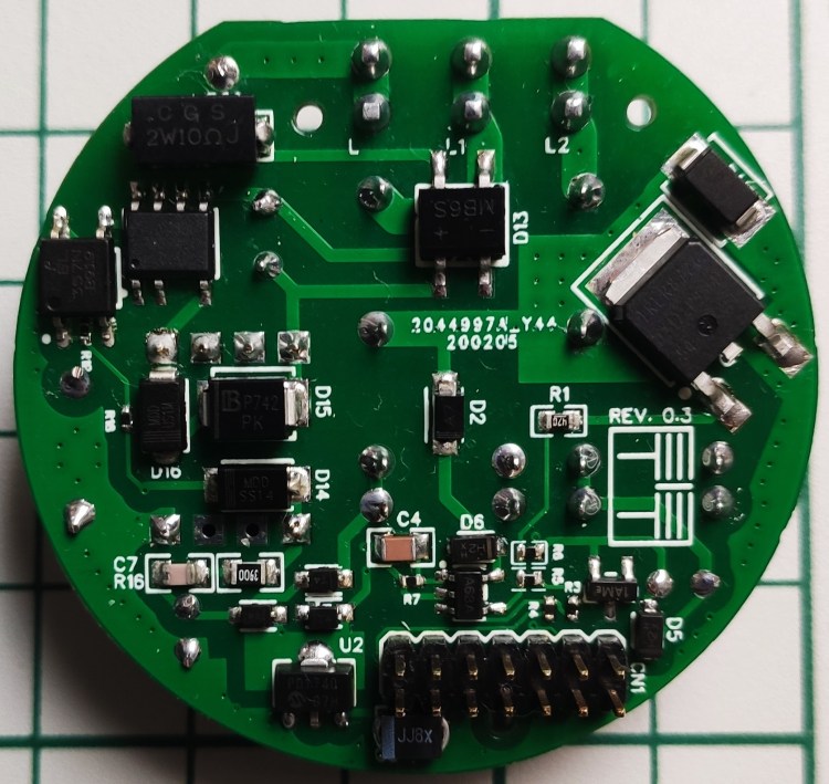
And yes it borrows the dimensions and more or less the layout of the original Livolo board as I needed to make it fit in the wall and also be compatible with the front plate.
Overall I was extremely happy with this design and especially with the stuff that I also learned by doing it which is much more valuable.
Limitations
Yes there are limitations for this design as nothing is perfect.
One is the fact that this power supply gets its juice via the light bulb so in some cases (if not the most) the bulb will flicker when the switch is turned OFF.
Why?
Because being in series it draws the current via the light bulb and in some cases it may be enough to determine the internal power supply of the light bulb to start working but it won’t be able to do it fully so it will oscillate causing the flickering.
The solution?
A bypass capacitor can be mounted across the light bulb. A 0.1 – 0.47uF / 275Vac capacitor will help to avoid the flickering.
The capacitor is not that big in size so it should fit in every light appliance from the wall or ceiling.
Other important things to consider:
- If the power supply will oscillate or restart sometimes when switching back and forth in the ON/OFF states then the MCP1703 LDO output capacitor must be increased – I settled to a B case tantalum capacitor and a 220uF/6.3V value but maybe it will work with a 100uF/6.3V value also. This happens because when the board will switch from the stand-by power supply to the series regulator circuit and vice-versa there must be enough energy stored in the main capacitors: C2, C3 and C5 so that the latching relays get enough power to do their transitioning in a 20ms interval (this is set by the relay manufacturer and can be found in the datasheet as the minimum pulse length to trigger the relay). We also need power for the front plate during this time of course. And yes, the B case tantalum capacitor will fit in the existing footprint from the PCB.
- The inrush current limiting resistor (R20) was a little bigger than I expected so the footprint on the PCB was smaller but it can be soldered over one pad and then the other pin can be soldered over one of the main fuse pins which it connects to.
The final design including schematic, Gerber files and BOM can be found on my GitHub page here.
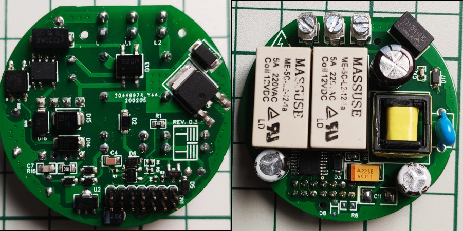
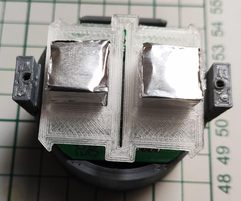
The final design and assembly
This is for the 2 channel variant (there’s also a 1 channel design):

Happy hacking!

Hey, loved the write up!
Just wondering if there’s any references as to how low a load (without the cap across the load) you can use without any ghosting flickering? Have you done any testing?
Chhers
LikeLike
Hi, thanks. I did some testing with low wattage bulbs but still some required a capacitor so no luck. It depends on the electronics inside the bulb in the end as well. And as I explained in the posts this is a tricky situation to power a load hence the issues and challenges.
LikeLike